contact
3rd Floor, Nanhai Plaza, NO. 505 Xinhua Road Xinhua District, Shijiazhuang Hebei China
+86-311-86935221
+61-0417-264-974
[email protected]

Diy Flexible PCB - How To Make It

  • High Temperature &High Density Applications; Saving On Space and Weight
  • Quality assured with more Reliability & Durability
  • Flexible PCB Lead time:Usually 5-6 days(depends on your special design)

Diy Flexible PCB
capabilities

  • Placer Speed:
    6000 Chips/Hours
  • Lead time:
    25+Days (To Be Decided)
  • SMT:
    SMT, Through Hole Assembly Single / Double-Side SMT, Single / Double-Sides Mixture Assembly.
  • PCB Size:
    50 mm×50 mm ~450 mm×406 mm
  • PCB Thickness:
    0.5mm~4.5mm
  • Min. Diameter / Space of BGA:
    0.2mm / 0.35mm
  • Qualifications:
    ISO 9001:2008
  • Accuracy:
    <±40 µm, Under the Condition of 3σ,CPK≥1
  • Min.Line / Track Width:
    3mil
  • Minimum Width / Space of QFP
    0.15mm / 0.3mm, Minimum Diameter / Space of BGA: 0.2mm/0.35mm
  • Reliability Test:
    Flying Probe Test / Fixture Test, Impedance Test, Solderability Test, Thermal Shock Test, Hole Resistance Test, and Micro Metallographic Section Analysis, etc.

Diy Flexible PCB
process

Double-Sided Flex PCB

  • 1
    Cutting
  • 2
    Drill Hole
  • 3
    Electroplate
  • 4
    Pro-Processing
  • 5
    Dry Film
  • 6
    Chech Position
  • 7
    Exposure
  • 8
    Development
  • 9
    Graphic Electropating
  • 10
    Etching
  • 11
    Decorating
  • 12
    Surface Processing
  • 13
    Cover the film
  • 14
    Press
  • 15
    Solidification
  • 16
    Immersion Nickel
  • 17
    Printing Character
  • 18
    Electrical Measurement
  • 19
    Puncing
  • 20
    Final Inspection
  • 21
    Shipment

Single Panel

  • 1
    Cutting
  • 2
    Drill Hole
  • 3
    Dry Film
  • 4
    Check Position
  • 5
    Exposure
  • 6
    Development
  • 7
    Eching
  • 8
    Decorating
  • 9
    Surface Processing
  • 10
    Cover the film
  • 11
    Press
  • 12
    Solidification
  • 13
    Immersion Nickel
  • 14
    Printing Character
  • 15
    Shear
  • 16
    Electrical Measurement
  • 17
    Puncing
  • 18
    Final Inspection
  • 19
    Packing
  • 20
    Shipment

Diy Flexible PCB
Lead Time

Flexible Circuits (1-2 Layers)
5 ~ 8 Days
2 week Standard Lead
Multilayer Flexible Circuits (3-6 Layers)
7 ~ 15 Days
3 week Standard Lead

Diy Flexible PCB
cost

WellPCB Start to serve Flexible PCB Manufacturing with a very Competitive Price.

We have already finished the R&D of 1-4 layers flex and rigid-flex board and passed the test. We can provide some unique requirements of rigid-flex boards.

pourquoi nous

Experienced & Professional

  • We provide highly experienced manufacturing personnel to work with your challenges and technological needs.

Fairly Fair Price

  • Our price is one of the most competitive in the world
  • Own factory with good cost control, no hidden cost in it
  • Accept T/T, cash, credit card, PayPal, bank transfer, etc.
  • Our two factories have price support for different orders

On-Time Delivery

  • Common methods are DHL and FedEX, door-to-door service. Normal Shipping Time only 2-4 Days.
  • Cooperate with two transportation companies for many years with discounted prices
  • Anti-static+Moisture-Proof+Anti-Vibration Packaging; Inspection certificate
  • Professional agent To Iran, Pakistan

Quick Turnaround

  • We specialize in quick turnaround with critical delivery schedules.

Return and Refund

  • In case our PCB is not usable due to our fault, you can ask for compensation.
  • We can refund to your account directly or rework the unusable boards or re-fabricate your PCB and re-ship to you at our cost, but please cooperate to solve the problem if need to rework.

Products Show

Testimonial

NXP France

Contact us

Flex PCB prototype is also referred to as flex circuits are made up of a thin polymer film that is used for insulation. 

It also has conductive circuit patterns that are fixed to it. 

There are different types of flexible circuits like the double-sided

metal layer and the rigid-flex circuits that are made up of circuit boards both in their internal and external.


The following content is more detailed

[contact-form-7 id=”47680″ title=”Contact form 1_copy”]

Flex PCB Prototype-How To Make It

Table of Contents

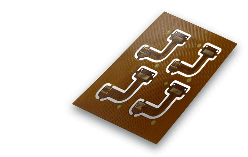
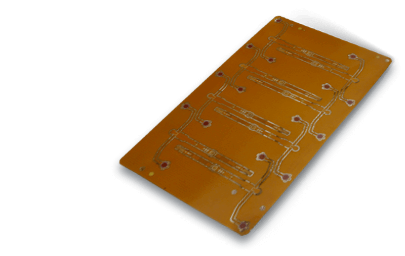
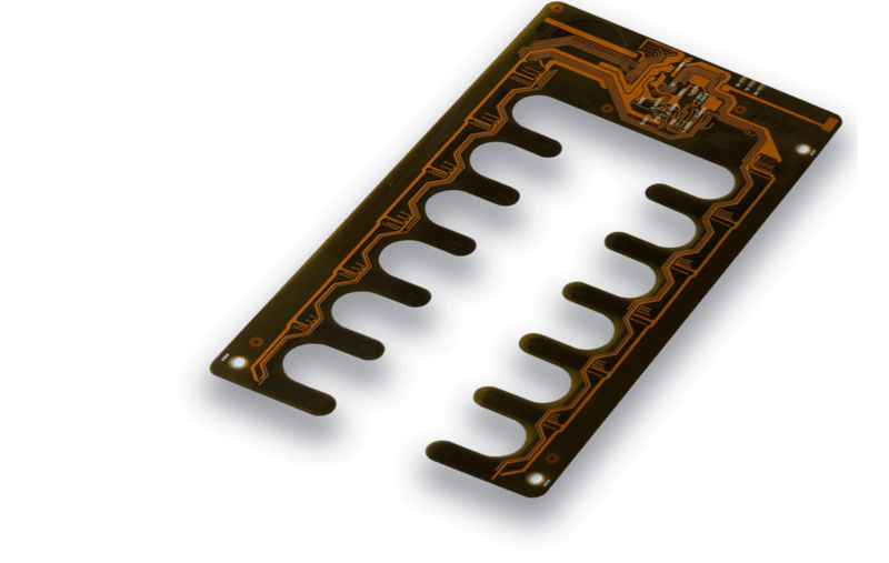
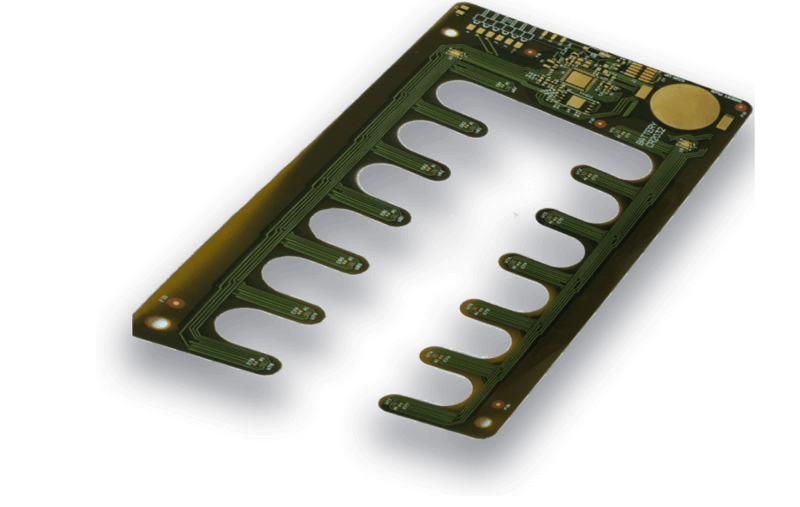
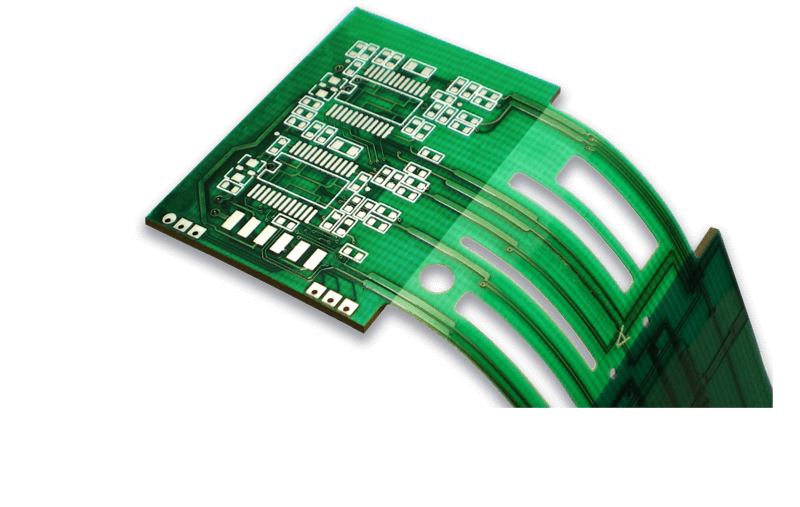
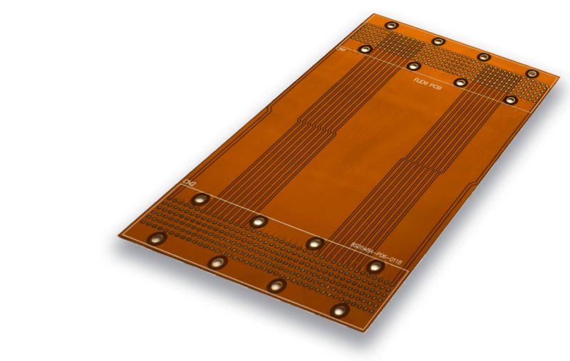
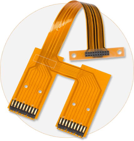
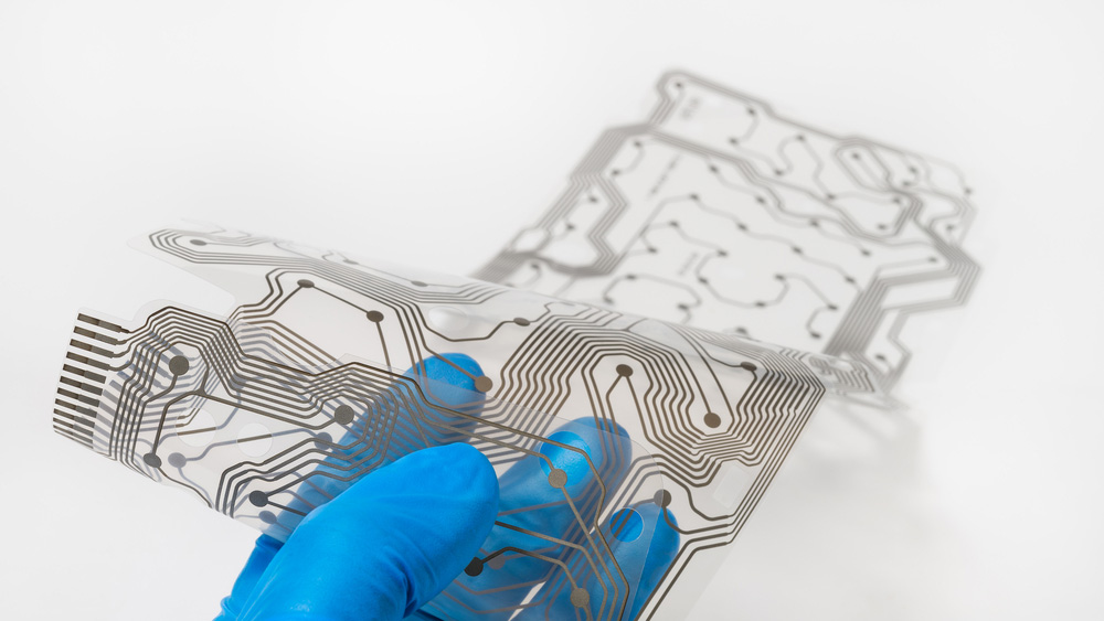
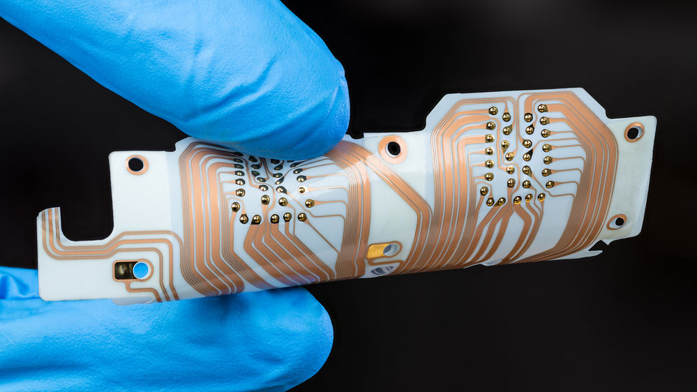
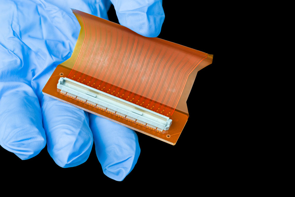
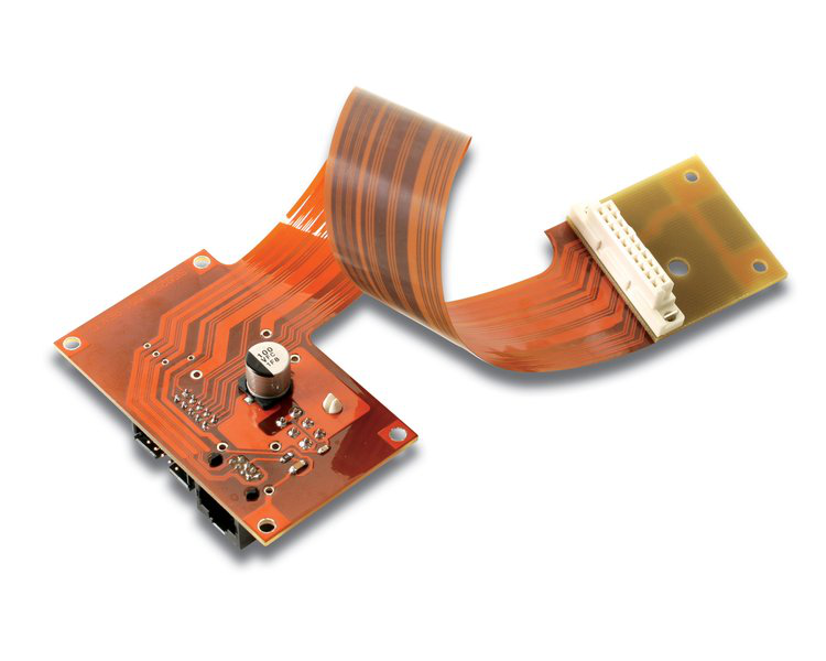
Flex PCB prototypes, also referred to as flex circuits, comprise a thin polymer film used for insulation. It also has conductive circuit patterns that are fixed to it. There are different types of flexible circuits like the double-sided metal layer and the rigid-flex courses made up of internal and external circuit boards.

YouTube video

flex pcb prototype2.png

1.Basic steps of making Flex PCB Prototype at home

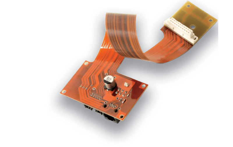
One can make a single-sided flexible circuit that is printed using a copper-coated polyimide film, solid ink printer, and the etching chemicals for a standard circuit board. Flex PCBs are primarily found in cell phones or gadgets of that kind. These flex cables are used for making tiny cables and very lightweight circuits. One should follow the following steps in making these flexible circuit boards:

1.Make use of copper-coated film.

Get the thin polyimide sheets that are made up of copper on both sides. Polyimide is a polymer characterized by a yellow color and a high melting point.

2. Use a solid ink printer.

When printing directly to the copper film, find a solid ink printer mostly confused with the laser printers that print wax that is melted. The wax is meant to make a protective layer that is good for copper etching. The printers from solid ink do not rely on charging the paper’s surface locally like the laser printers, which could cause trouble when the copper sheet replaces the form. In this step, one can replace the iron-on method toner transfer while using the design of a laser printer instead of a solid ink printer.

3.Print on Pyralux.

Draw a design in a graphics program and use a manual feed tray to print on your sheet of parallax in black. Avoid the shades that are light which are made up of tiny dots on the white background. The areas that are printed are protected by wax. When printing, use ‘photo’ or ‘high resolution.’

4. Etch it. Place the sheet that is printed in ferric chloride for around five minutes.

The time for etching will depend on the levels of temperatures and the thickness of copper. Wait for the areas made of copper to dissolve and the film of polyimide to show up.

5. Populate the board.

At this point, the flexible PCB is ready to be cut into small circuits and solder. It can be taped on metal or a circuit board made of fiberglass to hold it steady while working on it.

2.Advantages of Flex PCB Prototype

♦ Flexibility. Their flexible nature makes them suitable for electronic devices that need three axes connections, requiring minimal wiring.

♦ Saves on weight and space. Flex PCBs save space and weight up to 60% as compared to wire applications.

♦ Anti-vibration advantages. Due to their light nature and flexibility, the circuits can absorb and reduce the vibration impact.

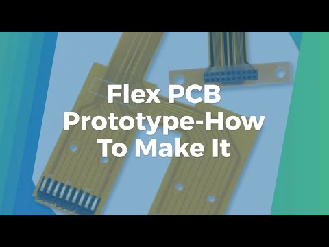
You can also check this video:

https://www.youtube.com/watch?v=j3vBrYjtvmY

flex pcb prototype3.png

3.Flex PCB PrototypeConclusion

In conclusion, flex Electromagnetic Interference (EMI) is responsible for many cases of circuit board failure. EMI causes about 50% of PCB prototypes to be an integral part of our day-to-day lives due to their diverse sizes, shapes, and functionalities. If you want to get high-quality flex PCB within a short time frame, you can contact WellPCB. They are a renowned manufacturer from China who also offer customization of the products.

Circuit Board Fabrication and PCB Assembly Turnkey Services

Online Quote Contact Us