We will test all the boards before shipping to ensure all of the printed circuit boards are free of defects and meet the standards you expect. Currently, we have two different types of testing equipment available to test the circuit boards. Some test machines include a flying probe, fixtureless testers. And we also have universal grid testing capability. These machines use fixtures built specifically for your PCB. If you have impedance control requirements, we will also test the impedance value of the coupon.
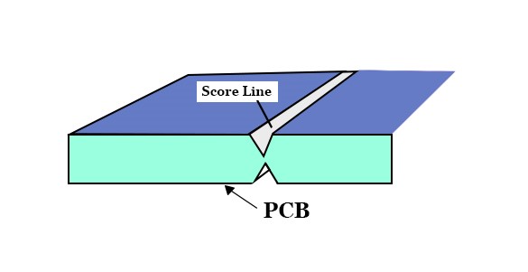
Here, we route the PCB production panels into particular sizes and shapes according to the production file. PCB V-Scoring is a process of cutting a ‘V’ shaped groove at the top and bottom of a printed circuit board, leaving a thin layer between the Vees. Once we have done this, it can easily separate the PCB Board at the V by applying minimal pressure.
In this step, a team of sharp-eyed individuals scrutinizes each product. The process involves visually examining the board in line with the set standards.
We pack your products by neatly wrapping them in materials that meet international packaging standards. Then we ship them through your preferred transport mode, mainly by DHL, FedEx, UPS, etc.


NXP France
Every day, people depend heavily on electronic devices to get things done around the house and at their job places. These devices help us cook, clean, and do a host of other activities that would have been difficult or impossible to accomplish without them.
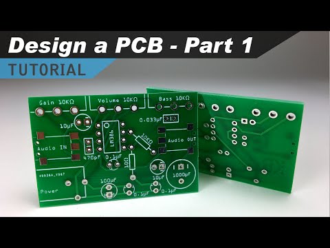
At the heart of every electronic is a printed circuit board (PCB). A PCB is a board that connects various electronic components in a particular device. So how do you choose a PCB that perfectly meets your specific needs?
This friendly guide has all you need to know everything about a custom circuit board and where you can get the best custom circuit boards for your needs.
The Basics You Should Know About Custom Boards
1.1: PCB Prototype Board
In the first phase of developing a custom board. It is much simpler to use a board designed for prototyping. Keep in mind that the fabrication and design of PCB will be required when it comes to adding the final touches to the end product.
1.2: PCB Material
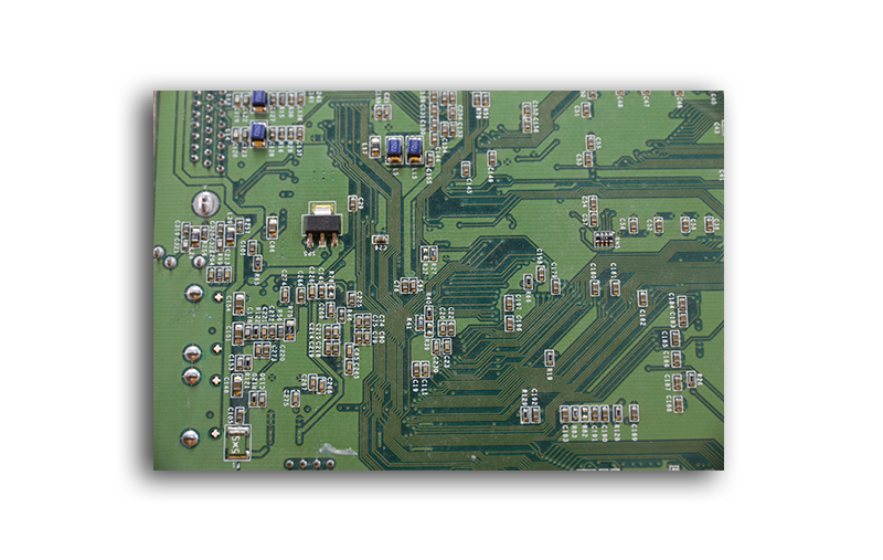
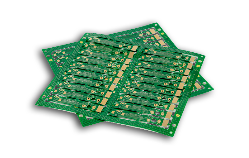
Some of the materials needed for creating a custom circuit board include the copper clad board as well as the positive photoresist. The copper gathers on a foundation that’s referred to as the substrate. Designers can choose between one and two layers of copper, depending on what type of board is in use. There’s a silkscreen that helps make the PCB readable. The substrate, usually known as FR4 (Fire Retardant), works as a thick foundation for the PCB. On top of the copper foil is a layer that’s referred to as the solder mask. It’s usually green in colour.
Some PCBs do not use these materials. Instead, they use epoxies, which have the disadvantage of being thermally sensitive.
1.3: PCB Types
PCBs come in many types, depending on the intended use. The most prevalent custom circuit boards include:
1. Single-sided printed circuit boards
2. Double-sided PCBs
3. Multilayer PCBs
4. Rigid PCBs
5. Flex PCBs
1.4: Printed Circuit Board Components
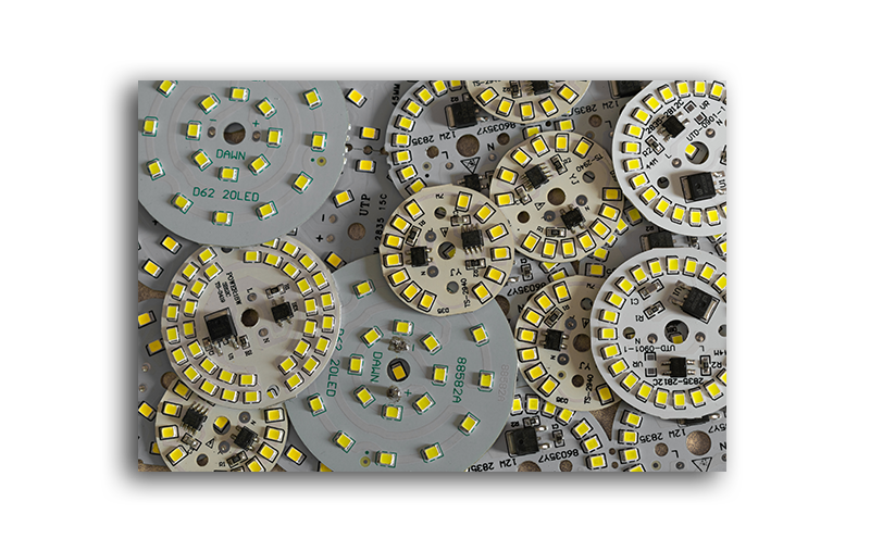
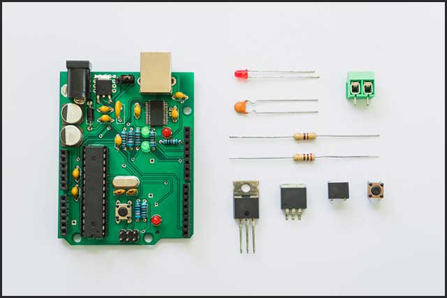
All electronic components, regardless of their function, have individual components that are essential for various circuits. These components include LEDs, resistors, battery, transistor, switch, diode, and inductor.
How is the Custom Circuit Board Designed?
2.1: The Design Basics
Before we get started on the basics of custom Circuit Board design, we need to get familiar with some terminologies. These include:
2.1.1 Schematic Capture
It is a program that allows the operator to create a schematic diagram of the electronic component as well as other features. In other words, it’s a graphical representation of the element.
2.1.2 Gerber Files
These are computer-aided design files. The files are sent to the custom circuit board producers to assist them in building the PCB structure.
2.1.3 PCB Layout Tool
It is a program that allows for applying on multiple structures of the wiring connection structure. Once the construction is complete, the operator can then generate CAD files to be used to make the custom circuit board.
2.2: The Steps of PCB design
Different makers of printed circuit boards use different approaches when it comes to the designing of a custom circuit board. We’ve listed the essential steps below:
Step 1: Using of Software
Here, the designer chooses a suitable software to create a custom circuit board. One such software is EAGLE.
Step 2: Generating the Film
Using the finalized PCB diagram, the operator generates the film.
Step 3: Selecting Raw Materials
Where the intention is to design a simple device, the designer can use pocket-friendly material like paper phenolic that’s bonded with copper foil.
Step 4: The Drilling of Holes
Machines and drill bits help to drill holes at this stage. Both a hand machine and a CNC machine are applicable here.
Step 5: Fixing the Image
Here, the designer places a clean copper layer on the printer and stores the designed layout film on the computer before they print the command from the computer using a laser printer.
Step 6: Etching and Stripping
In this stage, the unwanted copper that’s attached to the custom circuit board is removed using different chemicals.
Step 7: Testing
It is the final stage, and it’s meant to ensure that the custom circuit board is fully functional.
Do You Know The Custom Circuit Board Software?
Currently, there’s a wide variety of software available in the market to help design custom circuit boards. Among the top software include: PCB Artist, Altium Designer 17, Ultiboard, DipTrace, SOLIDWORKS PCB, PCBWeb, BSch3V, Gerbv, XCircuit, Eagle PCBs, KiCad EDA, CircuitMaker, DesignSpark PCB, Pad2pad, ZenitPCB, OrCAD, CircuitStudio, PCB123, FreePCB and CUSPICE
3.1 Comparing Various PCB Design Programs
As you’ve seen, the list of software used for PCB design is long. We’ll pick two programs from the catalogue to compare. Of course, we can randomly select these two applications. Let’s take a look at DIPTrace and EAGLE CAD.
3.1.1 DipTrace
This software has many impressive capabilities. The program can perform schematic captures linked to the library. The software can also create patterns using a decent library editor. Users of this program can access tutorial and support. The software is also reasonably priced and has visually appealing colours. Generally, this software is ideal for small and simple custom circuit boards.
3.1.2 EAGLE CAD
This software is capable of electrical rule check, and forward and backward annotation between the PCB and schematic.
3.2. So what’s The Best Custom Circuit Board Design Software?
Given that there’s a great deal of circuit board design software in the market, putting your finger on the best among them is easier said than done. However, some design programs are highly recognizable due to their impressive functionality. One of them is EAGLE. This software is remarkably user-friendly and comes at a moderate price. The software can perform the batch execution of files as well as copper cladding.
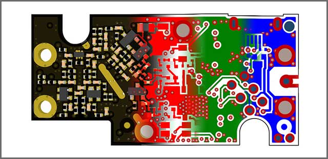
Custom Circuit Board Layout Design
4.1: PCB Layout Design
The layout of a printed circuit board requires you to have some technical know-how and calls for the knowledge of software used to make PCB. You also need to be conversant with the computer-aided system used to make PCB, as well as have the skills required for the transfer of the basic PCB design to the final custom circuit board.
4.2: Comparing PCB Layout
When comparing various custom circuit board designs, we look at the following factors:
1. Board size
2. Layers available
3. Power delivery network
4. 3D modelling
5. Differential pair routing
4.3: PCB Layout Tutorial
Step 1: Converting the Schematic to a PCB
Once you have completed the schematics, click on “convert to PCB” on the specific editor you’re using. Doing so converts the schema to PCB.
Step 2: Dragging and Dropping the Component
Here, you place the document to the exact position you want it. If you prefer a neat looking custom circuit board, you can set the components that have a similar function next to each other.
Step 3: Sketch a Custom Outline
Here, you need to go to the layer menu and select the board outline layer. Then you click on the outline and delete it. Next, create your preferred shape using the printed circuit board tools.
Step 4: Copper Area
This step involves joining different parts to one signal. You can create a copper area with the tools menu.
Step 5: Routing
There are two ways to complete the route. Where there’s low current where you’re creating the custom circuit board, use the auto-router function at the top of the page to do it. Where there’s the need for different track sizes, it’s best to do routing manually.
Step 6: Holes
Irrespective of what you’re designing a custom circuit board for, you’ll still need to mount it on something. To create holes on the PCB for this function, use the Hole tool on the tools menu.
Step 7: Adding Pictures and Text
To add pictures and text onto the PCB, go to the tools menu, and stroll to find the text or picture tool. Position your preferred book or make changes as you wish.
Step 8: Photo View
As soon as you’re through with the above steps, it’s the time to view the result. In case you’re not happy with the colour or some other feature, you can change it. If you’re satisfied with the final result, click on “fabrication output.” That helps you buy the custom circuit board.
Printed Circuit Board Reverse Engineering
Sometimes, the schematic is not available. In such cases, you can produce replacement parts using the data created from the PCB reverse engineering. Reverse engineering a custom circuit board can be a tedious and challenging; process, but it still has to be done at times.
5.1 Why We Reverse Engineer PCBs
So why would we bother to reverse engineer circuit boards, given the time and effort involved? Well, here are just some of the principal reasons:
- To replace components on the PCB that have become obsolete
- Reposition some of the board components
- To improve the functionality of the circuit board
- Analyze and enhance security requirements
Conclusion
Given the enormous role that printed circuit boards play in electronic devices, the PCB you choose must be ideal for your needs. At the beginning of this article, we’ll tell you what’s involved in creating a custom board. I hope this information will help you. We also promised we’d help you find the right vendor for you. That’s where WellPCB comes in. When it comes to reliable, cost-effective, and durable products, you can count on us every time. Our PCB solutions are customized to fit your unique needs.
Would you like to discover more about our high-quality products? One call is all it takes! We have the best, and it’s all for just you.