


On Printed circuit Board Blind Vias, Are you looking for more space in your extremely packed PCB design? Are you tired of drilling so many holes through your PCB? Did you know that there could be a way to design your PCB other than the standard way?
We know of a way where you would not need to increase your PCB board size or the layer count. You can enhance your multilayer PCB’s capacity from top or bottom, wherever you wish to. Blind vias on PCBs are such PCBs where you don’t need to make a connection using a through-hole. In this guide, we will tell you all that you need to know about producing a PCB with blind vias. Buckle up, so much more valuable information is coming in the next sections!
1. Blind Vias
We are sure that you can’t wait to know about PCBs with blind vias. How can they help you with your projects? However, first, you need to know about vias and how they are related to printed circuit boards (PCBs). It is only then that you will be able to understand the blind vias easily.
1.1. What is a Via?
Vertical interconnect access, via, is made up of two pads aligned in parallel places on different layers of PCB design. A hole then makes these layers electrically connected. The hole itself is electroplated or copper-plated, and that is what makes them conductive. In plain English, vias are these electroplated holes in PCBs that permit the layers to make an electrical connection.
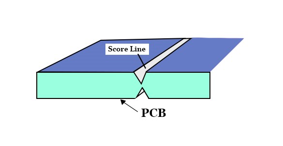
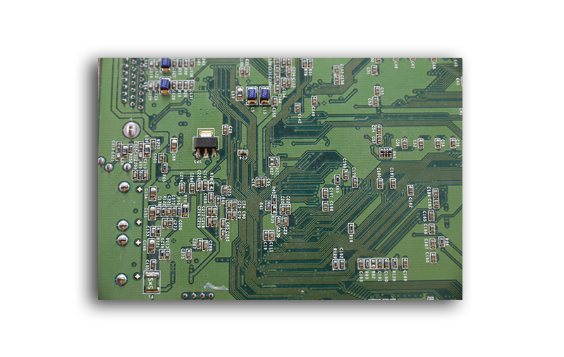
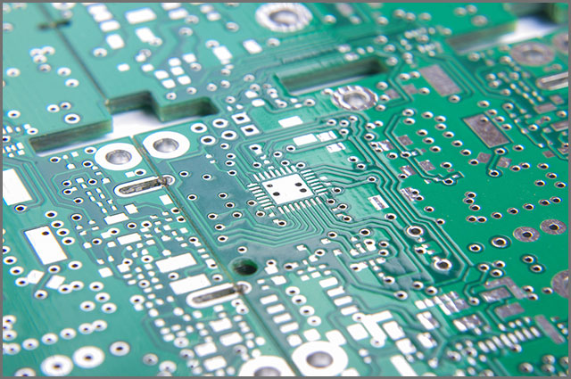
A typical via comprises of a barrel, a pad, and an anti-pad. A barrel is a conductive duct that fills the bored hole. A pad is responsible for connecting both ends of the barrel with the plane, electronic component or trace. Finally, anti-pad is the leeway hole present between the barrel and its unconnected metal layer. Figure 1 illustrates the via copper-plated holes on a fragment of PCB.
Vias is a valuable asset for proficiently making modern day complex multilayer PCB designs. Moreover, these PCBs usually have a small size and are extremely occupied by electronic components. Vias can be categorized into four different types, i.e., Stub via, Blind via, Through via and Buried via.
Stub and Through vias are almost similar to each other. Through via goes through all the copper layers but does not make a connection with any internal layers, whereas, a Stub via can make a connection with any internal layers. A Through-hole via is also known to be the standard via.
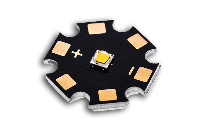
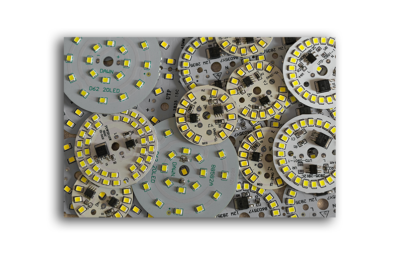
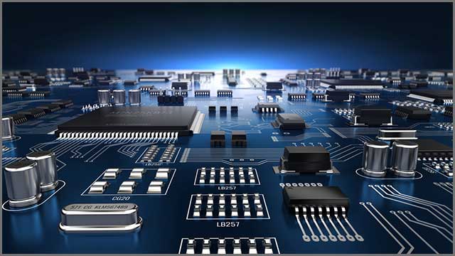
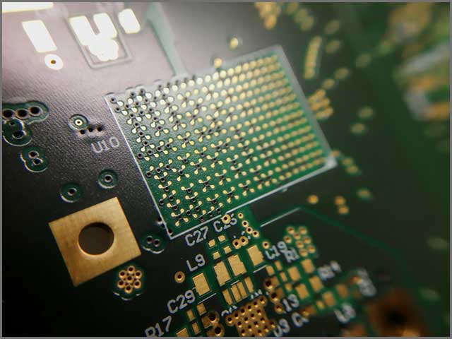
However, Through-hole via is known to have many disadvantages when used in Surface Mount Technology (SMT). It is the main reason behind why you should use buried or blind vias instead. Figure 2 shows a modern day high technology PCB with lots of surface mount components.
1.2. What is a blind via
Blind via is an electroplated aperture that starts from the surface of PCB, connecting an external layer with internal layers. The external layer is always one and can be either top or bottom surface of PCB. On the other hand, inner layers can be one or more than one. Thus, the specialty of blind vias is that they are visible only on one side of the printed circuit board.
The aperture never pierces through the board; make sure that you don’t make it go through the entire circuit board. Furthermore, it would help if you always started boring the hole from either the top or bottom layer. Hence, they are called blind vias. For piercing the blind vias, you can use laser or drill.
Now let’s get to why PCBs with blind vias are used? They will be your knight in shining armor when you don’t have enough space on the bottom or top of your PCB, or you cannot drill a hole on one side simply because the other side of PCB is already extremely packed. Coming to designing the blind vias, you will define them in a separate drill file. Complete details are coming in the next chapters.
2. PCBs With Blind Vias
2.1. How are the standard PCBs made?
The standard procedure for making PCBs follows these three basic steps:
1.The Substrate material is made and is stacked in layers;
2.For plating the vias, through-holes are drilled; and
3.Copper trace modeling is done using etching and photolithography.
If you already know about this procedure, you would know that it offers limited via configurations. You can only make through-holes vias. However, more via types can be achieved using drilling methods that can control depth such as lasers.
Normally, PCB manufacturing begins with a core, the first two-sided PCB. Layers past the first two are piled or stacked from this fundamental building block. Then, different configurations are possible by drilling at every stacking or piling stage. Furthermore, you must collect information from the PCB manufacturer about the permitted techniques of stacking and the potential via types.
If you buy inexpensive PCBs, keep in mind that you will be only able to drill through-holes. After that, anti-pads are put on layers which are supposed to remain isolated from the vias.
2.2. How are the PCBs with Blind vias made?
PCBs with blind vias follow the standard procedure of making multilayer PCBs, only till the drilling stage. They offer extra holes that make a connection between only two layers if the PCB is four-layered. Before starting the PCB designing procedure, decide what build-up are you going to use and check with the PCB manufacturer.
If you are someone who considers adding vias ‘on the go’; you may have to face dire consequences. Your PCB space will run out and eventually; you may have to discard the board and re-design everything. Furthermore, it will waste your time, energy and money. So, to save you from these consequences, we will describe in detail how to add blind vias to your PCB.
Before going forward, we will mention the basic rules that all blind vias must follow:
- The must begin from either the bottom or top layer of the printed circuit board.
- The must occupy an even number of layers, i.e., 2, 4, 6 and on.
- They should never go through the whole printed circuit board.
- They can never begin or end at the center or core of the PCB substrate.
Recall that blind via in the printed circuit board, with multiple layers, makes a connection between the surface layer and internal layers. However, due to certain limitations, it is a complicated task to drill a blind according to the modeled depth. For good plating or metallization quality, via sizes should be correctly selected
The hole depth to hole diameter, H/d value, should not be greater than 1, and 0.8 is ideal value. Thus, the deep vias should have large diameters. Moreover, huge vias also mean that the dielectric gap between PCB layers is also huge.
To properly make the blind vias, you would need to first bore the vias in the center cores. Then, make the vias go to the surface layers of PCB. In the end, prepreg assists in stacking together the PCB layers.
In conclusion, we will say that you must compare your circuit requirements with the processing abilities of PCB manufacturer. Additionally, PCB manufacturers have often mentioned rules that must be followed to make PCB producible. Thus, it is good practice to learn about the design rules of blind vias, as provided by the PCB manufacturer.
2.3. Applications of Blind vias
In this section, we will discuss the two main applications of Blind vias in PCBs. First, you can decrease the number of layers in your PCB by broadening the ball grid array breakout channel. How could you do that? The answer is simple – make blind vias!
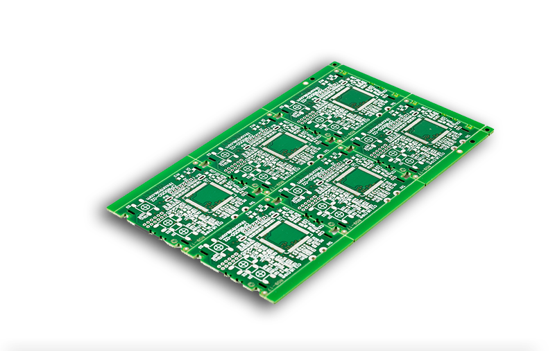
You may be drilling through-holes vias for modeling and trace escaping of ball grid array (BGA). Is it going smoothly? If not, try broadening the breakout channels on the inner and bottom layers using blind vias. Figure 3 shows a BGA traced on a printed circuit board (PCB).Secondly, you can decrease the PCB aspect ratio using the blind vias. Frequently, BGA components in a PCB have many different pitches. For instance, on a 4.0mm thick PCB, there could be a 0.8mm pitch BGA and a 1.27mm pitch BGA. The Minimum size of via hole doesn’t only depend upon the drill proportions, but also on the aspect ratio of PCB.
The aspect ratio of PCB is given by:
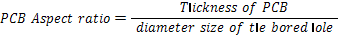
Blind vias will decrease your PCB aspect ratio by reducing the number of layers in it. Simply substitute through-hole vias with blind vias.
2.4 Features of PCBs with Blind vias
In summary, following are the clear-cut features that you will observe in PCBs with Blind vias:
1.They will have more holes than a traditional PCB. If the PCB is four-layered, the extra holes will only join two layers.
2.They will have higher pad density and wiring than traditional PCBs.
3.There will be reduced trace space and width.
4.During the fabrication process, they follow a slightly complex build-up process.
5.They are an inexpensive solution.
Amazingly, there is another very beneficial type of vias – the buried vias. In the next chapter, we have discussed it in detail and have compared it with blind vias.
3. Buried Vias
3.1 What is Buried vias?
Similar to Blind vias, buried vias also make a connection between layers. The layer count should be even, i.e., 2, 4, 6, 8, and on. However, the distinct difference between buried and blind vias is that buried via only connects the inner layers. Thus, they never join the outer layers, i.e., the bottom or top layer of PCB.
Therefore, buried vias are always inside the printed circuit board; you cannot see them from the outside. And that is also why they are called buried vias. Further, buried vias are also electroplated holes, and they also need a separate drill file.
3.2 How are the PCBs with Buried vias made?
The procedure for making the buries vias in a PCB is similar to blind vias’ procedure, except that buried vias should remain invisible to the outer layers, i.e., keep them buried. To develop a Buried via, you should make the needed traces and then stack up to the inner layers as usual. After that, develop the vias and test them. Finally, you would need to stack up the external layers to make the whole PCB package. So, this package will have buried vias squeezed in between.
4. Blind Via PCB Design Limitations
4.1 10 layer Blind via PCB
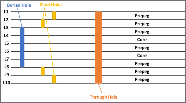
Underwriter laboratories say that for supreme quality and reliability, you should not produce PCBs that need over three lamination steps. It means that you should not design vias such that they need more than three steps for assembly. This issue arises when you are dealing with PCBs having more than six layers.
Figure 4 shows an example of a 10-layer PCB that would need two lamination steps. The first step, drill the buried holes and electroplate them from layers 3 to 8. In the second step, drill the blind holes and electroplate them on their layers and then laminate the rest of the layers. In the end, drill the through-hole vias and electroplate them, but this is not a lamination step. Hence, this PCB board only requires two lamination steps and three drilling steps.
4.2 Costs of Blind via PCBs
As already mentioned, blind vias in printed circuit boards can decrease the layer count and aspect ratio of PCBs. But how is it beneficial for you? Hold on! These two very things have the potential of reducing your overall WellPCB. We will provide you with one-stop service and high-quality products. You can send us the documents you need to make and get a quote immediately! What are we waiting for? We have ten years of PCB manufacturing costs. Furthermore, there are generally extra manufacturing charges if your PCB aspect ratio is more than 10 or 12. So you can avoid any cost penalties and save money simply by using Blind via PCBs.
5. Blind Via In Altium And Eagle
5.1 How to control Blind via in Altium?
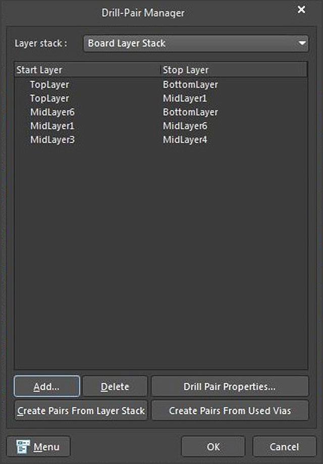
Select a via and click on the properties panel to open the “drill pair manager” in Altium Design. Then add the drill pairs as this is how Altium will know that blind vias are in use. It will also specify the starting and ending layers of blind via. Figure 5 shows the Drill-Pair Manager window. Carefully define the start and stop layers, then click ok and close the manager. Altium will get your design configuration.
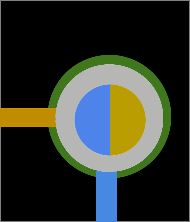
Altium will show you the blind vias in two colors to define the starting and ending layers. For example in Figure 6, blind via starts from the blue colored layer and ends on the yellow colored layer. Moreover, after placing the blind vias, you can still edit them or move them around.
5.1 How to set up Blind via in Eagle?
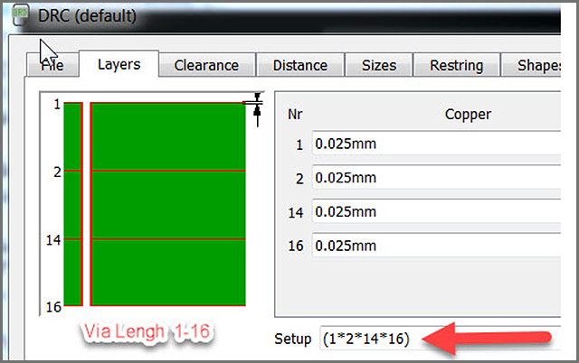
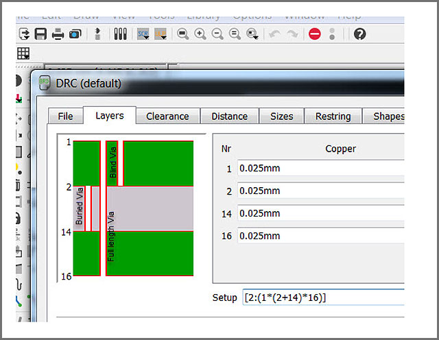
You would need to open Design Rule Checker (DRC) settings by clicking on Edit/Design Rules in Eagle. In DRC, go to the layers tab and add the blind vias. Figure 7 and 8 shows the example of 4-layers set up in Eagle. In the pictures, setup values are according to the configuration of layers.
Conclusion
Now, are you thinking of using blind vias in your PCB design? We would recommend you to stand by your decision and discover the world of PCB blind vias. In this article, we have included everything that you need to know about blind vias. You don’t need to visit other links.
Furthermore, if you still need more help or want to ask something, we are always here for you. Simply contact us at [email protected] or visit our website to get the best customer support. Our team of Engineers can easily handle the complexity the blind vias need and provide very high-quality work.