Various problems may occur during PCB fabrication Problems. Knowing how these problems arise is important since it helps deal with those problems long before they occur. This brief discussion will prepare the PCB engineer ahead of time.
1. PCB fabrication problems-The Vias
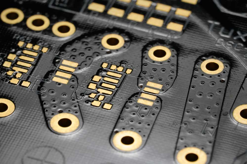
PCB fabrication, desired holes for vias are drilled on the PCB using a thin cutter or laser cutter. To make vias, the holes are then plated to become conductive. During this plating, process discontinuities come about. When the conductive copper layer doesn’t adhere to the PCB’s cylindrical inside surface, the PCB Design will have discontinuities (gaps) and develop other unique problems in your PCB. This may not be easy to troubleshoot. This problem is often caused by rough drilling or fast drilling, which causes the hole’s internal structure to break, rendering the hole defective for an even and uniform copper deposition.
The solution to this problem is to ensure that you always drill a smooth hole before a via is made. This means using the recommended tool and applying the right force for the hole drilling.
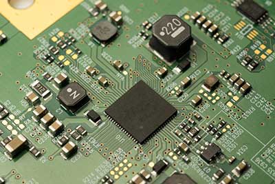
2. PCB fabrication problems-Missing solder mask
This is another common problem that affects most PCBs. When the pads’ space is too small, the solder mask will not be deposited between the closely packed pads. This will make the PCB vulnerable to short circuit and during the assembly and testing process. This problem also shortens the life of a PCB since it will be exposed to oxygen and moisture, which are good ingredients for rust. SMD pads for microcontrollers are the most vulnerable.
The solution to this problem can be taken care of during the PCB design stage in the software. Again, this is achieved by sticking to the manufacturer’s recommended clearances, copper trace, and the size of the copper pads. This keeps the traces and pads spaced out, and the copper mask will readily rest between the pads.
