


NXP France
10 Common PCB Quality Problems You Should Know
Abstract
On 10 Common PCB Quality Problems, PCB assembly is much correlated to the PCBs Quality of PCBs design and its manufacturing. As every PCB design engineer tends to place and route components according to his own design tactics. Similarly, all PCB manufacturers do not have an equal manufacturing facility, skilled manpower, and raw materials. When putting PCB design rules in practice and manufacturer the boards. There are certain key design issues and aspects to look for before pursuing to design finalization and fabrication.
Table of Content
1.Copper thickness
2.Discontinuous Vias
3.Solder mask voids
4.PCB Warpness
5.Surface finishing
6.Bad impedance
7.BGA solder void
8.Poor cutting and dimensioning
9.Blurred Silkscreen
10.Improper internal layer connections
1.Copper thickness:
The copper thickness on a PCB is important, especially for high current applications. A thin track for high current applications may behave like a fuse. High current tracks need more copper thickness and vice versa. The PCB manufacturers are to ensure the finished or base copper thickness as per the design requirement.
It is checked after finished PCB finalization, either by destructive test or microscopic test of the copper tracks. It is mentioned in ounces per inch on the board surface i.e. The weight of copper in per square inch of the lamination sheet. Common copper thickness is 17, 35 and 70µm thickness. Along with copper thickness. The etched and finished copper width is also important and mandatory to maintain.
2.Discontinuous Vias:
The vias connect one layer to another. In PCB via manufacturing process. They are fabricated by using machine drilling or laser drilling. The holes are made conductive by depositing a thin metallic conductive layer by the electroplating process. They are called plated through hole vias. Too fast hole fabrication or electroplating causes. It to broken and causes partial or full discontinuity. It causes various problems in PCB Quality testing or product failure.
The through-hole vias, blind, buried ad micro vias in multilayer PCBs are more prone to connecting. External layers are more prone to fault and tedious to troubleshoot. This problem can be solved by adopting an advanced speed compliant via fabrication technique. Or incorporating vias with the large hole and annular ring sizes. (The figures Fig 1 and Fig 2 depicts very common problems of via manufacturing.)
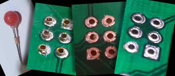
Fig 1:- Different type of vias and cracks on the annular rig surface of the via.
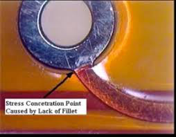
Fig 2:- Copper track to via connection breakage due to lack of fillet
In dense PCBs, when manufacturing via-in-pad. It is hard to get the via and pad annular ring pad totally flat without some sign of a dimple on the surface of the pad. This can give the assembly house problems during soldering and testing. It is particularly hard to correct with leadless parts such as BGA and QFN packages.
3.Solder mask voids:
This is a common problem in PCBs manufacturing. The solder mask layer which is required for copper exposure to open environment saves copper and vias by corrosive effects. It also mitigates solder bridging during PCB soldering and assembly. The solder mask voids do arise when two footprint-pads are designed very close to each other.
Solder mask cannot be deposited in the free area between two pads. The solder mask, in its existence, resists the solder bridging. This problem causes the PCB susceptible to short-circuiting and failure of PCB within Lab. The solder voids are more dangerous for PCBs designed for BGA package components.
This problem can be avoided by taking care of the PCB designate PCB design rules definition design stage and sticking with PCB manufacturer recommendations.
Figures Fig 3 explains the solder mask voids in the PCBs.
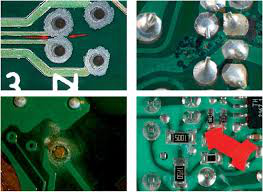
Fig 3:- (top-left) too much less solder mask clearance defined in PCB design rules
Ensuring that solder mask layer properly joins the edge of each pad, not too much distant and even does not overlap. It will ensure there is no exposed copper. Exposed copper in component pads will cause the bare boards to pass electrical testing (E-test) at the board manufacturer. In-house PCB Quality control, but once solder is used to solder the component. It may bridge the exposed copper between pads and cause a dead-short.
4.PCB Warpness:
Also referred to as PCB twist and mostly arises in multilayer boards. It occurs due to lack of temperature control and heat unbalanced increase rates during manufacturing of the board. A good manufacturer will control heat increase rates. Also, provide necessary rigid support to the boards to ensure flatness during manufacturing. PCB warp once occurred during manufacturing is almost impossible to remove. PCB warp also causes complete copper-tracks breakage or cracks.
The flatness is a visual PCB Quality aspect of the boards and generally conducted after finalizing the manufacturing process. Or before PCB Quality control stage prior to assembly. During components mounting and assembly process the flatness of board is important for solder paste deposition and components mounting. However, it is also important during manufacturing to handle and position the boards accurately.
To prevent PCB warp, the PCB manufactures adopt different techniques. For example, a PCB manufacturer bakes the PCB panels in an oven with the temperature set to 260°F (degree Fahrenheit) to keep the boards flatten. It seems to remove some of the former lamination warp. As the press under high temperature heats up the laminate cores become more pliable, causing the etched conductors to revert back to its actual size and initial position.
The common practices exercised to mitigate PCB warp in the industry during fabrication are to select the base material which is suitable for lead-free soldering, low elasticity, and high rigidity, and sustain rigidity during the whole board fabrication process. Use proper temperature, pressure ad pressing materials to reduce stress till board finalization. Avoid mixing materials of different types and from different manufacturers. Use appropriate heat-ovens for temperature provisions and cooling chambers for proper processing.
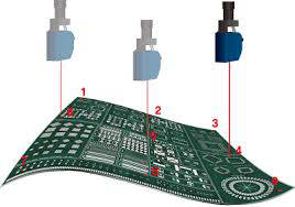
Fig 4:- A 3D model of PCB warp (bow and twist) of a manufactured PCB
5.Surface finishing:
The surface finishing or surface smoothness of PCBs like pads, vias, via-in-pads and copper tracks is also very important. Most of the PCB manufacturers commit and guarantee good PCB Quality. ENIG (Electroless Nickel Immersion Gold) surface finishing and used mostly.
ENIG contaminations impose extreme difficulties in soldering. Because the surface particles and impurities act as a barrier to build a joint between the footprint-pad and component pad. The subsequent lab testing reveals the decreased pull strength. Even if the component looks soldered properly. However, the problem of the improper joint building still exists.
6.Bad impedance:
The impedance, faced by signals traveling from the source to destination in a PCB. Is an important parameter for high-speed digital (such as the motherboard) and RF (mobile phones) PCBs. The common problem found by the assembly houses is that the impedance differs considerably between different PCB lots causing impedance mismatch of product response difference. This problem can be encountered on PCB manufacturers end by using proper PCB base and pre-preg materials and improving etching techniques to improve track
7.BGA solder void:
During PCB assembly the BGA pads solder voids may lead to the dry joint of the chip and hence poor performance of the board assembly. It is possible that it may not be detected in the boundary test or lab performance test. So it is necessary for BGA package soldering companies to have affixed the X-RAY inspection setup. In figure Fig 5, the BGA package component is shown with solder void and its detestation using X-Ray inspection setup.
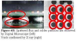
Fig 5:- BGA package solder void and inspection
8.Poor cutting and dimensioning:
The size of a PCB in an assembly is very critical for many reasons. The PCBs should be ensured and guaranteed to be compliant with dimensional sizes and tolerances sought by the designer. It is much critical to fix them inside the mechanical box or assemblies. It becomes even more serious when it is required for very compact multi-part assemblies like industrial applications. The board cut with too large size or too small size may not fit into the mechanical box assembly. The mechanical dimensions of a PCB quality are checked visually before proceeding to assembly.
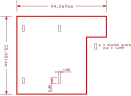
Fig 6:- Finished PCB dimensional cutting
9.Blurred Silkscreen:
For components, PCB nomenclature marks, layer count and other assembly marking are generally placed in silkscreen layer of the PCB. A poor or low-resolution printing machine may cause poor blurred character printed on the PCB. It causes misinterpreted designator numbers. For an instance, it is hard to differentiate between 1 and 7, and B and 8 characters placed on poorly printed silkscreen PCB.
10.Improper internal layer connections:
It is a very common problem among PCB manufacturing and utilization industry that internal layers of the PCBs such as signal layers, ground planes, and power supply planes are short-circuited. This is quite undoable and very hard to locate the problem. The PCB quality problem can be identified by using effective E-test methods.