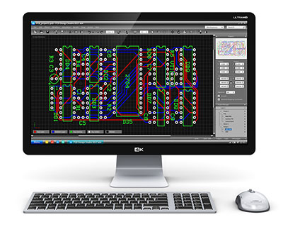
Electronic circuits have been around for a long time now, and like any design, modeling is essential for manufacturing the end product. PCB layouts and other circuit designs need to be precise, accurate, and flawless for the manufacturer to create an effective and efficient final product. Speed is similarly essential in designing schematics at the end of the day. Your business needs to make a profit. This article aims to provide a comprehensive and detailed tutorial on how to download Ultiboard, create a circuit, and maneuver around the platform to export the design for manufacturing. We hope that this will be beneficial.
1. What is an Ultiboard?
Ultiboard, formerly known as ULTIboard, is a program created by Ultimate Technology in the Netherlands. It was pretty expensive as it would go for $800–$2500 depending on the size required. Additionally, the affordable version for students was limited in the market.
Over time, Ultiboard developed from a program that could barely produce photo plot files to when it was known as Electronics Workbench and now Ultiboard. An advanced platform with schematic capture and simulation tool-Multisim facilitating users to easily design PCB models, manipulate than to products ready for the manufacturer.
1.1Function
Ultiboard is mainly used for its benefits:
- Easy to use and efficient PCB layout program- routing tools for PCB designs; customizable and accessible features
- Optimum control and management of the environment- Ultiboard has an advanced spreadsheet view, toolbox, design wizards, and other tools improving functions such as copper placement and the general board layout.
- Transfer of simple schematics to PCB- Ultiboard integration with Multisim™ provides features and tools that facilitate precise placement of parts as well as automated functionality for the fast working of the layout design.
- File Standardization-You can export your design file in one format such as DXF or Gerber to another format that is required for standardization purposes.
Ultiboard’s main objective is to provide flexibility regarding control, efficiency, and speed in layout, routing tools, and copper placement. It is used by engineers, manufactures, students as well as teachers in different environments. Let us look at how we can get access to Ultiboard, how to download and install it.
2. Ultiboard download
Instead of downloading Ultiboard and later during installation, realize your system lacks several requirements. Generally, to install Ultiboard 9, you require about 150mbs. However, this varies depending on the version you need. Also, your system should at least have:
•Windows 2000/XP
•Pentium III Processor
•128 MB RAM
•CD-ROM
•800 x 600 screen resolution
You can get the version of any Ultiboard professional or academic product on the National Instruments website. The installation is simple and similar to most application installation processes. Having installed Ultiboard, you need to get familiar with the software interface to interact with it optimally. Our next will focus on essential to standard components that you need to identify before you begin designing.
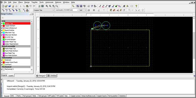
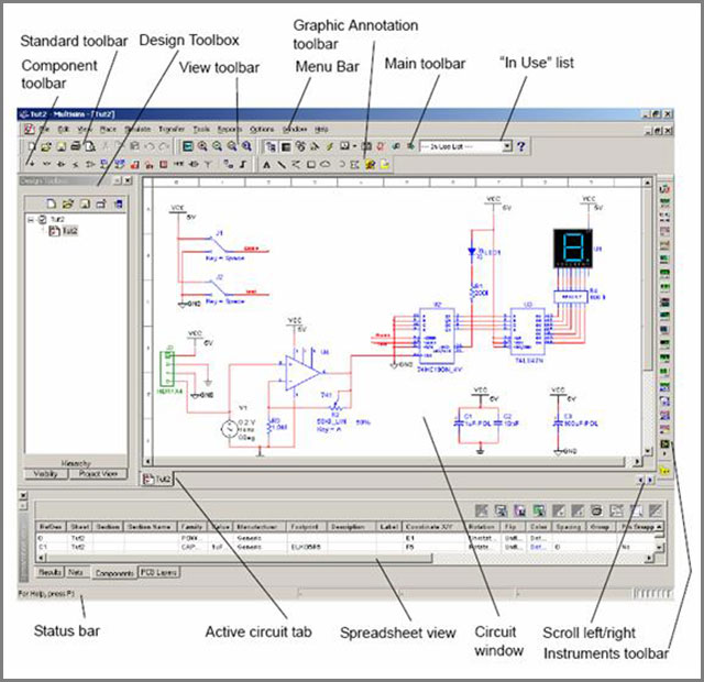
3. User Interface
3.1 Introduction to the Ultiboard Interface
The Ultiboard interface combines tools and features that aid you, the user, to maneuver around in designing your circuit or PCB layout. It facilitates the creativity and innovation of new and original designs that will improve the electrical products industry. Ultiboard interface offers a platform for mechanical parts placement in creating your PCBs, manually designing CAD operations to their manufacture.
The user-friendly interface has brought speed thanks to the automated functionality. Also, precision can be achieved by placing parts in the correct position due to manual control. Together with Multism, Ultiboard results in generations of further advanced and better-performing PCBs. Why? Mutism compliments Ultiboard PCB layout and routing abilities through its powerful SPICE simulation functionality. You can get started with your design in no time.
3.2 Toolbars
If you have used any common application such as MS word, Ultiboard toolbars will not be rocket science. Most of the symbols are ones you are already familiar with; in case of any new ones, you can hover around the icon to know their function. Nevertheless, here is a guideline:
Main toolbar
 Select icon –Select an element from the board.
 Design Toolbox icon –‘Switches’ the Design Toolbox view on and off
 Spreadsheet View icon –‘Switches’ the Spreadsheet view on or off
 Database Manager icon –Displays the Database manager view
 Board Wizard icon –Start Board Wizard
 Part Wizard icon –Launches the Part Wizard
 The place from the database -Browse the database for a position to place an element
 Line icon –Place a straight line on the design
 Follow-me icon –Place a follow-me trace
 Polygon icon –Places a polygon on the design
 Power plane icon –Places a power plane on the design.
 DRC and netlist check icon –Runs the DCR (Design Rule Check) and Netlist Check; It displays the results in the Results tab
 Text icon –Places text on the design
 View 3D icon -Displays the design on display in three dimensions.
 Capture screen area icon – Captures a section of the screen and places it on the system clipboard.
 Help icon –Displays the Ultiboard Help window.
Edit toolbar
 In-place part edit icon –Activates In-Place Edit for placed PCB parts
 Swap layer icon –Places a part or element on the mirror layer
 Rotate 90° clockwise –Rotates selected item clockwise
 Rotate 90° anti-clockwise –Rotates selected item anti-clockwise
3.3 Setting Preferences
To set your setting preferences:
- Click on the Options/Global Preferences for the Preferences dialogue box to appear, which will provide you with the options:
- General Settings Tab
- Paths Tab
- Colors Tab
- PCB Design Tab
- Dimensions Tab
- 3D Options Tab
2. Having selected the desired tab, go ahead and customize or edit the details.
3. Click OK to save your changes
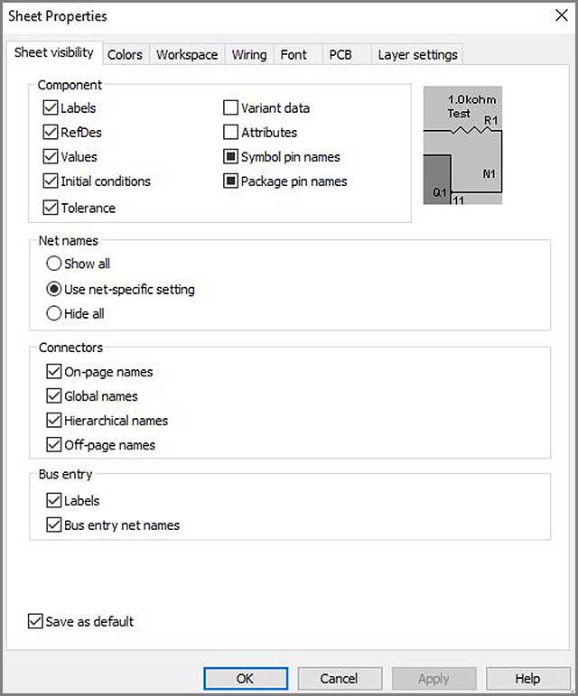
3.4 Setting PCB Properties
To set the settings of the PCB properties:
On an empty board, right-click to display a menu box and select the property icon. The Sheet Properties dialogue box will appear where you can further edit your PCB details as desired.
3.5Design Toolbox
You are most likely to use the Design toolbar to manage your design in controlling parts, such as determining the colors of a trace. To display or view it, click on the Design Toolbar.
3.6Spreadsheet View
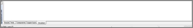
The Spreadsheet view is essential in viewing and editing details such as attributes, footprints, or Reference Designators.
To access the Spreadsheet View icon, you have to have a new project open. Once you click the icon, the functionality tab will appear at the bottom of the pages, with several buttons/icons.
However, not all tabs have all the icons.
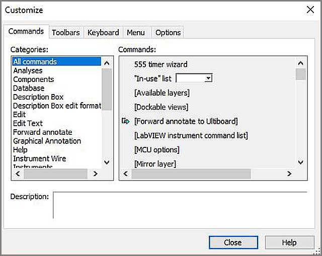
3.7Customizing the Interface
To customize your interface:
Select Options/Customize User Interface to display a menu tab below, where you can make changes as desired.
We have covered the fundamental orientation steps of customizing Ultiboard to your liking and using different icons. Therefore, our next step will be to learn how to design a simple schematic and further employ more features and properties of the software during the process.
4. Ultiboard Design Tutorial
4.1 The Electronics Workbench Suite
It is an EDA suite that facilitates significant steps in designing a circuit. Depending on your requirements and budget, you will have some of the components of the Electronics Workbench Suite, such as:
- Mutism: it is a combination of the Muticap and both analog and digital simulation capability
- Multicam: a schematic product for driving simulation, simple schematic and facilitating steps such as in Pcb layout designing.
- MultiVHDL: It brings on board co-simulation along with Multism and creation of HDL models.
- Ultiboard: a product that alongside from Multism and Multicap, is useful in the creation of PCBs and working on CAD operations mechanically.
- Ultiroute: an add-on to Ultiboard stand-alone, Ultiroute facilitate placement of parts on the design automatically.
4.2 Opening the Tutorial
To open the tutorial, ensure the Ultiboard is launched, then proceed to:
- Select on the Open/File icon. Go to where you stored your Ultiboard during installation (if you cannot remember to try the central disk C in the program files).
2. Open the Tutorial.EWPrj to load the selected file on the Ultiboard
3. To view a design, select it either by clicking the design tab or the Projects tab under the Design Toolbox
4.3 Creating a Board Outline
You can create a border outline in the following ways:
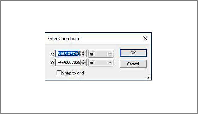
- Using the drawing tools- press the keyboard * and fill in your desired border outline coordinates:
• Import a DXF file
• Use the Board Wizard, which we will use in this tutorial:
- Along with the toolbar layer, go to the Border Wizard icon and double-click on it.
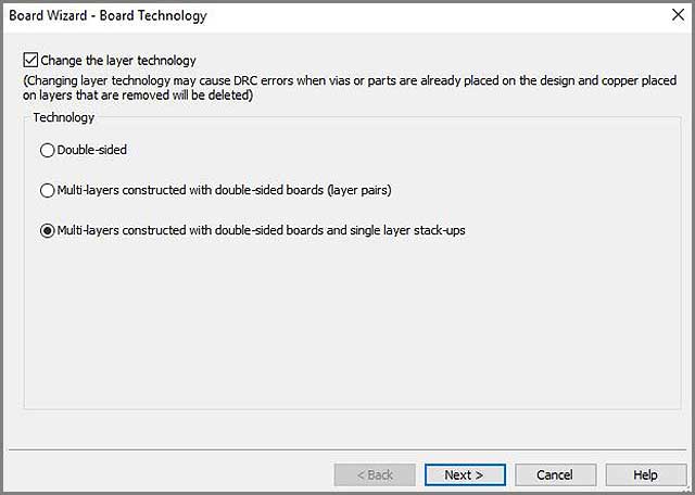
2. Delete the existing Border wizard in the current- it should be a new one for the Board Wizard-Board Technology box to appear.
3. Enable the ‘Change the layer technology’ to be able to select other options. Go ahead to choose ‘Multi-layers constructed with double-sided boards and single layer stack-ups, then click the Next tab.
- The next dialogue box is of Lamination Settings where you can make changes if necessary and click
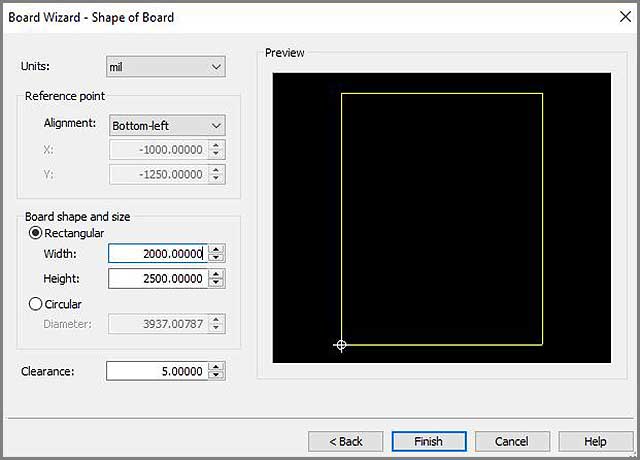
- The next Dialog box is the Shape of Board where you will make the changes as:
- Under the Reference Point, set the Alignment to the Left-Bottom
- Select the Rectangular for Board Shape and Size
- Set the Height and the Width as 2000 and 2500 respectively and the Clearance at 5.00000. Click Finish.
4.3.1 Ultiboard—Editing changes on the Border Outline
- To move the Boarder outline:
Double-click on Board Outline under the Layers tab. Proceed to click anywhere on the workspace border outline below the row of components.
- To make changes on the Reference point:
Click on the Options tab, place your cursor on the bottom-left of the border outline on the board and click to make changes on the box that appears.
4.4 Placing Components
You can place a component on the board by:
- Select a component(s) beyond the border outline and drag it in the desired position
- Go to the Spreadsheet View, use the Parts tab to locate a component(s), and place them appropriately
- Import component(s) from Netlist
- You can select the component(S) directly from the database
- Use the auto place
4.5 Placing Traces
There are a few ways you can put traces:
4.5.1 Placing a manual trace
Here, the trace is positioned where you place it. To do this:
• Choose the Line /Place command to create a line that depends on the layer (in the dropbox) where you place the tube.
• Click to anchor the trace and move the cursor towards the destination, where you will also click to anchor again or right-click to stop the drawing.
4.5.2 Ultiboard—Placing a Follow-me Trace
A follow-me trace allows you to draw a path between two pins you have selected by simply moving your cursor. It is achieved by:
• Click on the follow-my icon; ensure you have at least two appointed pins
• Click on one pin, then click on another pin for the Ultiboard to automatically draw the pin for you
4.5.3 Placing a Connection Machine Trace
The connection machine trace provides complete trace automation by joining two points through the most convenient route. It is achieved by:
• Click on the Place/Connection Machine icon
• Proceed to click on the space between the points you want to connect. Ultiboard will provide various route suggestions and once you identify the suitable trace, click to use it
• Right click to end the trace placement
4.6 Ultiboard—Preparing for Manufacturing/Assembly
Before submitting your designs for manufacturing, there are several activities that you can perform on the board to ensure you provide extra information or remove errors. They include:
4.6.1 Cleaning up the Board
That involves cleaning up open trace ends or any unused parts or connections. It is done by:
• Click on the Edit/Copper Delete/Open Trace Ends to delete all open trace ends.
• Click on the Design/Clean Unused Vias to delete any unused vias or connections
4.6.2 Adding Comments
Adding components provides extra information that the manufacturer can refer to or promote collaboration among team members. You can place a comment by:
- Activating the comment layer in the design box
- Select Place/ Comment and a dialogue box will appear as below:
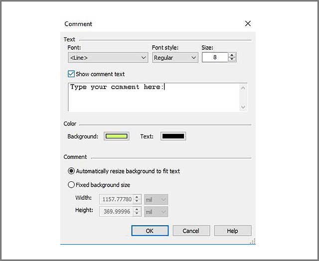
- You can choose to fix the background-size or make other edits such as the font style and size or text and background color.
- Type the comment as in the comment box
- Click OK. Proceed to double-click on the desired position for the comment to appear.
- To make any changes, go back to the comment dialogue box and edit any details as you wish and delete the previous comment that is not wanted.
- To delete a comment click on the comment and press the key DELETE
4.6.3 Ultiboard—Exporting a File
It is usually the final process that is producing your design as an output. It is transforming the design format to another that is understandable by the equipment of the manufacturer. The file contains detailed information on how the design should be manufactured.
The formatting requirements of the manufacturer mainly dictate the format. Exporting a file begins by pressing Ctrl-E or clicking the File tab, and a menu will appear, which is the Export option among the list.
An Export dialogue box will appear to view, export, or delete the export settings/properties.
4.7 Viewing Designs in 3D
You can view your design in 3D by:
Click on the 3D icon, which is listed in the Tools menu. A 3D preview tab will show displaying your design in 3D will show.
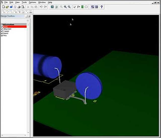
4.7.1 Manipulating the 3D View
- Click on the Tools bar then 3D to view the 3D preview.
- Proceed to click on the preview board and hold on the mouse/cursor and move to:
- Move the pointer of the screen to either side of the screen for a better or specific view of the board
- To pan the 3D wheel, hold down the cursor to view the four-headed arrow and point the desired direction
- To move the 3D view around, click and hold on it
- Proceed the pointer either direction to have a view of the design’s other sides; topo underside of the board
- To zoom in on an area: Click and hold onto the cursor and move/scroll it up or down
- Also, you can use the Zoom in/out under the View tab.
Hopefully, you can comfortably maneuver the Ultiboard platform by now and are familiar with different icons, tabs, and their property. Also, ultimately, you should create a simple design, as was our goal when we began.
5. Ultiboard—Advantages and Disadvatages of Using Ultiboard
1.Advantages of Using Ultiboard
- It is user-friendly and intuitive
- Can be integrated with other tools such as spreadsheet as well as used in managing constraints, copper routing, and part placement.
- It is easy to use and is optimized for speed
It can be exported to industry-standard including Gerber and DXF, for both manufacturing and prototype.
- Transfers schematic layouts since it is seamlessly integrated with Multism.
- It allows you to quickly gain insight into how to design your PCB.
- It annotates the changes made to the design.
2.Ultiboard—Disadvantages
Despite the many benefits that you get when you use Ultiboard, it is essential to note that it comes with many disadvantages. The most critical one is:
• It requires plenty of training to be able to use it.
• It is not a free tool, so you must be prepared to dig deep into your pocket.
3.Ultiboard—How it Works
When it comes to layout routing, choosing Ultiboard is recommended. Since it comes with an automated part and manual placement routing, the tools combine to reduce the time and effort needed in completing repetitive tasks. When combined with the placement process, it guarantees a quick layout. Ultiboard comes with trace placement that allows fast and efficient adjustment based on the complexity and the design.
It quickly finds and places components in the schematic since it comes with the pick and place functionality. It utilizes the follow me router and machines that input suggestions to the trace placement. When integrated with Multisim. It uses auto-routing, which allows the easy schematic transfer of layout reflected in many design versions. It, therefore, provides for the provision of an easy and quick flow of design and validation.
Conclusion
Finishing a design on a software platform is usually the first step to having a tangible product that works. Whether you are making an order for manufacturing or not, we at WelPCB are available for your questions, comments, or suggestions.
We offer cost-effective services on Printed Circuit Board Fabrication and SMT). This will make it easy for a pick and place machine to easily pick and place the components on the PCB (PCB Assembly Turnkey Services to meet the requirement of High Quality, Low Cost, Fast Delivery, Easy Ordering for customers all over the world. We are available 24/7 to chat with you. Contact us anytime from anywhere, and we will be glad to hear from you.
