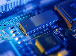
On Circuit Board Texture High Resolution, Modern electronics are becoming complex every day, and the need to make them compact is critical. Small circuit boards that host complex circuits are robust to implement and takes immense effort to design circuit board texture high resolutions. Unlike conventional printed circuit design and manufacturing processes, the high-resolution circuit board texture design and manufacturing technique vary across the manufacturers.
1.Circuit Board Texture High Resolution
High-resolution circuit boards textures are the same and function similarly to the conventional PCB. But, all of the connection lines and component placement are on the micro-scale. The high-resolution circuit boards are made with smaller trace width and shallow trace pad Clarence. Modern high-resolution circuit board textures are created with a trace of as low as 10µm. Modern compact electronics like mobile phones. Laptops make use of the high-resolution circuit board textures more.
As they are expected to be as thin as possible to make it sleek and compact. The design process of the high-resolution circuits board texture still stays the same as the regular circuit board. But, there must be design optimization to prevent any possible interferences in the high-speed digital circuit.
2.Manufacturing methods
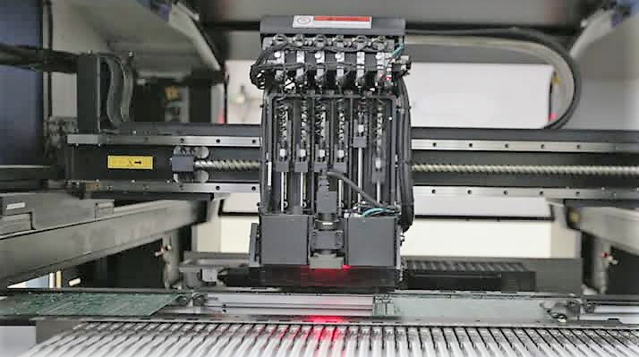
High-resolution circuits are a crucial feature of integrated circuits. As they are technically a circuit board in size, they have few millimeter areas. They are made by direct laser etching or hyper resolution mask etching methods. High-resolution circuit board textures are usually made with the same precision as integrated circuits. To make the photoresist small to cover a few micrometer thinness traces, UV light is passed through a high-resolution imaging plate rather than placing the image directly on the circuit board laminates. High precision CNC is used to do the milling and drilling process.
3.Practical difficulty
The primary practical issue in developing such high-resolution circuit board texture is the extremely trace width and clearance. The possibility of over-etching and improper masking is very high. The boards may suffer from unwanted solder brides due to the shallow working space. The next major challenge is the calibration of the CNC and assembly machines to perform the high-resolution machining. Signal compensation and length matching is also an issue at the microscopic levels. Low trace width also limits the current carrying capacity of the copper traces. Due to the concentration of typical width traces, these boards are fragile and easily damaged even to a very gentle impact.