How many times have you faced the problem of producing unreliable electronics due to a cold solder joint?
Did you get online help when encountering this issue in Industrial PCB assembly or prototyping with newer trends (like flexible PCBs)?
WellPCB, a PCB manufacturer, has often received worries about cold solder joints from customers. To give some insights on this topic and try to answer questions that could worry designers because of these concerns, we researched more for you!
This edition is a collection of information on cold solder joints that could help you develop better PCBs.

1. A Cold Solder Joint
1.1 First, What Is Soldering?
Soldering is the process of forming electrical and mechanical connections on a Printed Circuit Board (PCB) by connecting electronic components to the board using an alloy of molten Lead and Tin.
It is a fundamental skill in electrical engineering as it stands as a central part of developing and troubleshooting circuits.
Soldering is often done using a solder station or a soldering iron and a solder wire (the alloy of tin and lead). A subtle tip of metal (or a relevant metallic material) is attached to a controlled heating element connected to a power source during soldering.
With time, the solder iron tip gets heated to degrees that can melt the solder wire to become molten and aids in making a solder joint. Soldering is the skill that is responsible for mounting electrical components on PCBs.
1.2 Tell Me About Solder Joints
A solder joint is merely a specific soldered point of interconnecting an electronic component onto the PCB.
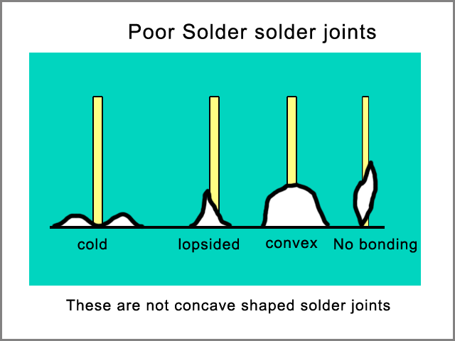
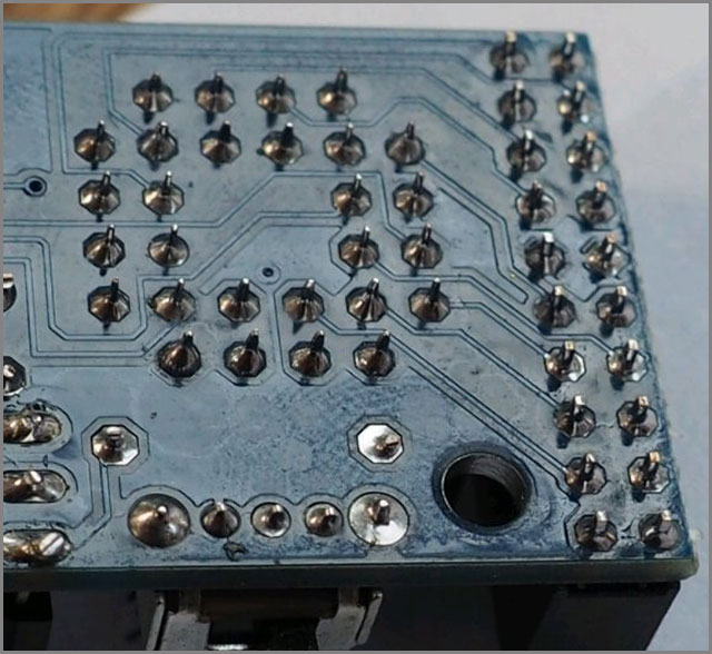
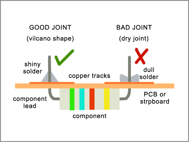
A cross-section of an ideal solder joint should have a smooth and glossy concave-shaped molten solder that climbs up the pin of the element that is to be soldered, as shown in image one below:
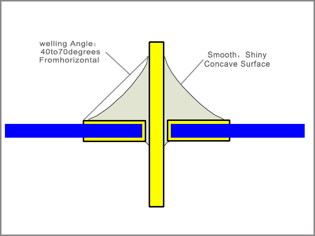
Image 1: the ideal solder joint
As you can guess from the simple explanation (or from experience), good soldering is an acquired skill that requires much practice. For most of us, this skill is perfected with time over repeated projects and experiments.
This learning process involves a lot of trial and error with lots of “…mount this,” “…unmounts that.”
Moreover, even then, you are never entirely free from error per se; you only become a little bit more improved than you were before the practice.
Meaning, every time you solder a component, you get yourself a chance to do it better than before or learn a better way to do it from a mistake you will make.
1.3 Common Solder Joint Issues
There are various mistakes you are likely to make during this process of soldering. Some of the common soldering mistakes you might make during making solder joints include:
1. A disturbed joint: formed when a solder joint is disturbed before the molten solder solidifies
2. A cold joint: one where the solder fails to melt entirely after soldering.
3. An overheated joint: this problem occurs when the soldering wire fails to melt despite heating. This act results in overheating the flux on the board, which complicates the soldering experience.
4. Insufficient wetting: This problem happens on either the pin or the board. It is an indication of not heating the solder unevenly on the board and the pin. Inadequate wetting of the pin shows that you burned the pin more than the board. Inadequate wetting on the board, on the other hand, could indicate the application of too little wetting material.
More about these issues will be explained in the other preceding chapters.
1.4 So Now, What Is A Cold Solder Joint?
I am sure you can now guess what a “cold solder joint” is as of now, can’t you? As already noted, a cold solder joint is a solder joint problem that often occurs during soldering when the solder fails to melt entirely and flow to form an ideal solder joint.
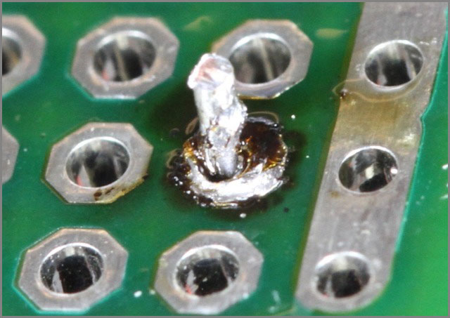
Cold solder joints often appear dull and make convex mounting on the pins and the board flex areas. Sometimes, they also take rough shapes, as shown in image 2.
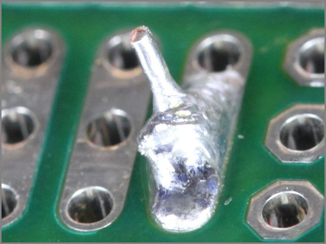
Image 2: a Cold Solder Joint
This cold solder joint often arises when one fails to heat the solder wire properly before soldering. In some cases, it can also emerge when one disturbs either the board or the soldered pin before the molten solder solidifies.
In the subsequent chapters, we will examine more details on detecting and repair cold solder joints.
We will also suggest practices that can help you to minimize the occurrence of cold solder joints.
2. Cold Solder Joint Detection And Testing
2.1 Why Should You Test For Cold Solder Joints?
Nobody appreciates the importance of testing for cold solder joints like one who works on large electrical projects.
Look, here is an annoying stage I do encounter when working alone on electronic projects.
I wonder if such a story relates to your daily work experiences too. It goes something like this:
I am working on an electrical module for a larger industrial project. My role is to develop one of the fundamental hardware components for the more massive project.
I already have the software and electrical component tested (on a regular breadboard) and uploaded onto a microcontroller, ready for soldering.
I gather my “tools of the trade,” and off I go grinding, trying to solder the whole stuff as fast as possible. About 30 minutes later, I get done with the entire project. Everything looks fine from my end (or so I should say).
So, I power it up and start monitoring it. Moreover, guess what? My circuit doesn’t work. “…well, maybe the resistor isn’t so well.” I think, “I was suspecting it earlier,” the thought crosses my mind.
So, I replace the resistor with a different one. However, still, it doesn’t work. I check for the multimeter and begin evaluating each component. I notice a single cold solder joint and fix it.
The device works, but then it gives unexpected readings. I get worked up and set for a new circuit examination using a lens. I later discover a different cold solder joint (after about another hour or so) and fix it.
This time I manage to bring it under control (after a long and tedious experience that might sometimes bring you behind schedule).
Do you see it? That’s the reason you need to check for cold solder joints. Without evaluating cold solder joints, you will run a risk of developing a defective electronic. With that said, let’s explore some of the tests you can carry out on circuits to establish cold solder joints.
2.2 Test One: Visual Checking Of Cold Solder Joints
Checking visually for cold solder joints and fixing them should be your primary step when developing circuits. We had already described how an ideal solder joint could look like (in chapter one).
Primarily, a cold solder joint could look dull, whitish, and convex, or deformed.
I know all this looks more like “common sense,” doesn’t it? Moreover, maybe you are wondering why I have introduced it. Sometimes it goes beyond what we see with our eyes.
You might need to get a magnifying lens and check through the solder joints to note the convex shape and that the solder filled the gaps. You shouldn’t be able to view light passing through the joints.
At times the lenses can help you detect those joints where the solder didn’t heat the solder enough. Often, such joints appear to be rough on a close examination.
Also, when you suspect a joint, you should try to tilt the component mounted on the joint to see if it detaches. Should such a thing happen, try and fix it with the methods we will discuss in the ensuing chapter.
It is also critical to ensure that the solder does not spill over to other joints as this could create short-circuiting within the circuit.
2.3 Test Two: Using A Multimeter to Check Cold Solder Joints
When testing for cold solder joint using a multimeter, there are two measures you can use to establish a cold solder joint. These are:
2.3.1 Testing by use of resistance (ohms)
Here you will begin by switching the multimeter to measure resistance. Often this will be indicated by the Ohm (Ω) symbol. Depending on the multimeter type, you will either rotate the indicator or press a few control dials to switch. Use a resistance of about 1K ohms for this experiment.
Next, you connect one terminal of the multimeter directly to the other terminal of the meter. Here it would help if you read a resistance of zero ohms. This step is to verify that your multimeter functions correctly.
Once you ascertain this, connect the meter’s terminal to a joint on one end and the other on a different end through a component. For non-resistor electrical components, you should observe a zero. Any reading above zero could be an indicator of a cold joint.
2.3.2 Testing by use of continuity
Using the same multimeter we used in test 2.3.1, switch the multimeter measure to gauge continuity. Connect the two ends of the multimeter and notice that the multimeter beeps to indicate continuity.
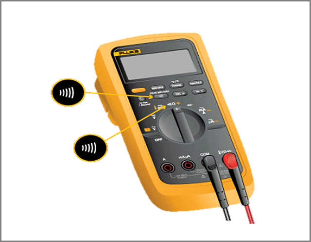
Image 3: Photo with an indication of continuity label
Once you are satisfied, repeat the process by connecting the two ends of the multimeter to the two ends of the circuit. If the multimeter beeps, then all could be fine. Anything else is an indication of a discontinuity that could be a result of a cold solder joint.
2.4 Keep this in mind: soldering mistakes are the way forward
No specific device can test for cold solder joints. All the tests explored above are based on trial and error. This fact is the reason why you should not fail to make mistakes when doing this. When you get too naïve to make mistakes with electronics, you eventually make mistakes.
Thus, you should do all this courageously and be willing to rectify anything you encounter (with the methods in chapter 3).
Over time, with more solved mistakes (that you make), you begin to become a little better than before. Just like a beginner makes mistakes, professionals make mistakes too.
The only difference is the type of errors and the amount of time they take to solve the errors. So, why should you be afraid?
3. Cold Solder Joint Repair
Cold solder joints often occur as disturbed cold solder joints or just cold solder joints due to the solder’s inadequate heating during soldering. We will begin with:
3.1 The Disturbed Cold Solder Joints
These are the main types of cold solder joint problems to engineers. These solder joints occur when either the component or the circuit board is moved before the molten solder mounts correctly.
They are characterized by a concavely shaped look and tilted pin within the solder. On a close observance, they are also likely to appear rough and a bit frosty.
Primarily, they cannot be comfortably classified as cold solder joints as this type of joint sometimes may be made from well-molten solder. However, they do exhibit a very close resemblance to standard cold solder joints.
Moreover, this is because the solder fails to cool appropriately before mounting electronics.
3.1.1 How to solve disturbing cold solder joints
As noted above, this type of cold solder joint is caused when one disrupts the board or element during soldering. Thus, you will need to work as you go on your soldering task steadily to solve this.
To go through this successfully, you might need to have a dedicated table mounted to the ground when soldering. If you work in a limited space, you can purchase a soldering vise and mount it on a solid wall close to a soldering station.
3.2 Cold Solder Joints
In the preceding chapters, we defined cold solder joints as being formed due to inadequate heating of the soldering material. Such a problem is readily observable as it leads to lumps close to the solder joints while failing to fix the components to the circuit board.
Because of this problem, the joint’s bonding may be very poor and might lead to the cracking or even disjoint of components attached to the solder joint.
Cold solder joints often occur when the solder gun is not supplied with enough power. Sometimes, it could as well be an indication of a “dirty” tip of the solder gun.
3.2.1 How to solve cold solder joint issues
For engineers using soldering stations, the only possible reason you could encounter cold solder joint problems is dirt that collects on the solder gun’s tip. This problem could also lead to overheating of solder joints.
Therefore, the first step to solving cold solder joints is to appropriately clean the tip of the soldering iron.
Secondly, you will need to supply the solder gun with an appropriate amount of electric power to heat the soldering wire. You will only need to adjust your solder station/ heater appropriately in some other cases.
After you confirm the heat, you will need to reheat the solder again and mount it.
In other cases, you might opt to consider buying lead-free solder like the SN96 solder that has a short plastic transition time. This type of welding will lower the chances of having incomplete combustion during soldering.
In the remaining chapters, we will discuss the soldering issues of joint resistance and its effects; then, we will crown it with recommendations of practices that could help you avoid cold solder joints.
4. Cold Solder Joint Issues
4.1 Cold Solder Joints And Resistance
In Chapter Two, we highlighted the test for resistance as a test for detecting cold solder joint. We missed the only thing that we expressed neither the reason nor the possible effects of the resistance on cold solder joints.
Now, it is important to notice that all joints exhibit some level of resistance to power within the circuit, however, due to the incomplete combustion of the lead and tin alloy solder substance used in soldering.
The cold solder joints may exhibit higher resistance to the flow of electric charges.
This problem is not always notable instantly. However, with time, it leads to more power consumption, and with prolonged usage, cold solder joints may overheat and eventually lead to device malfunctioning.
4.2 Effects Of Resistance In Cold Solder Joints
The high resistance due to cold solder joints is some “time bomb” for electronics. At times, the effects are instant, easy to notice, and easy to rectify. However, occasionally, the consequences might not be notable easily and could persist in producing defective devices.
Here are some of the effects that might result from cold solder joint resistance:
Incomplete circuits: This problem occurs when the cold solder joint fails to connect the component and the circuit. Though this problem is undesirable, it is the easiest to spot and rectify early enough as a device with this problem will not work.
In other extreme cases, the resistance might combine with other connected resistors’ resistance in the circuit to give erroneous readings. In such incidents, you can apply the already discussed testing methods and solutions to rectify this problem.
Overheating circuits: Overheating circuits occur when several different cold circuits are interconnected. It is the hardest cold joint resistance problem to detect. Most of the time, the circuits with this problem will work in the testing phase and might even be produced for industrial use.
The problem is that with prolonged usage, these circuits overheat and break the circuits for the electronics and consequently cause the gadgets to malfunction.
The best way to detect resistance issues caused by cold joints would be to use the multimeter to detect them, as discussed in chapter two.
Seven Soldering Practices You Need To Practice
Here are seven golden practices that could help you avoid the cold solder joint in your electronic projects.
1. Have the appropriate tools. More specifically, invest in a good soldering iron. The soldering iron is often responsible for the heating of the solder. Thus, it is essential to invest in an ideal soldering iron that can allow you to regulate and control the amount of heat used in soldering.
2. Use a minimal amount of solder when soldering.
3. Tidy the tip of the soldering iron regularly.
4. Have a reliable power source that can power the heater/soldering gun when soldering.
5. If possible, use the lead-free soldering wire (material).
6. Always give adequate time for molten solder to cool. Don’t be in a hurry to solder.
7. Never panic when soldering. I know this is not very necessary to already established engineers, but most beginners face cold solder joints due to panicking.
Conclusion
I have consistently highlighted the need to brave the soldering process as it is the primary cause of a cold solder joint. As we had seen before, you need to make some of these mistakes over and over again to be a little better than you were before.
To know more about soldering, feel free to browse through our website for more details.
Just in case you might need us to print you a reliable and professional PCB, feel free to make an invoice or an inquiry on our website.