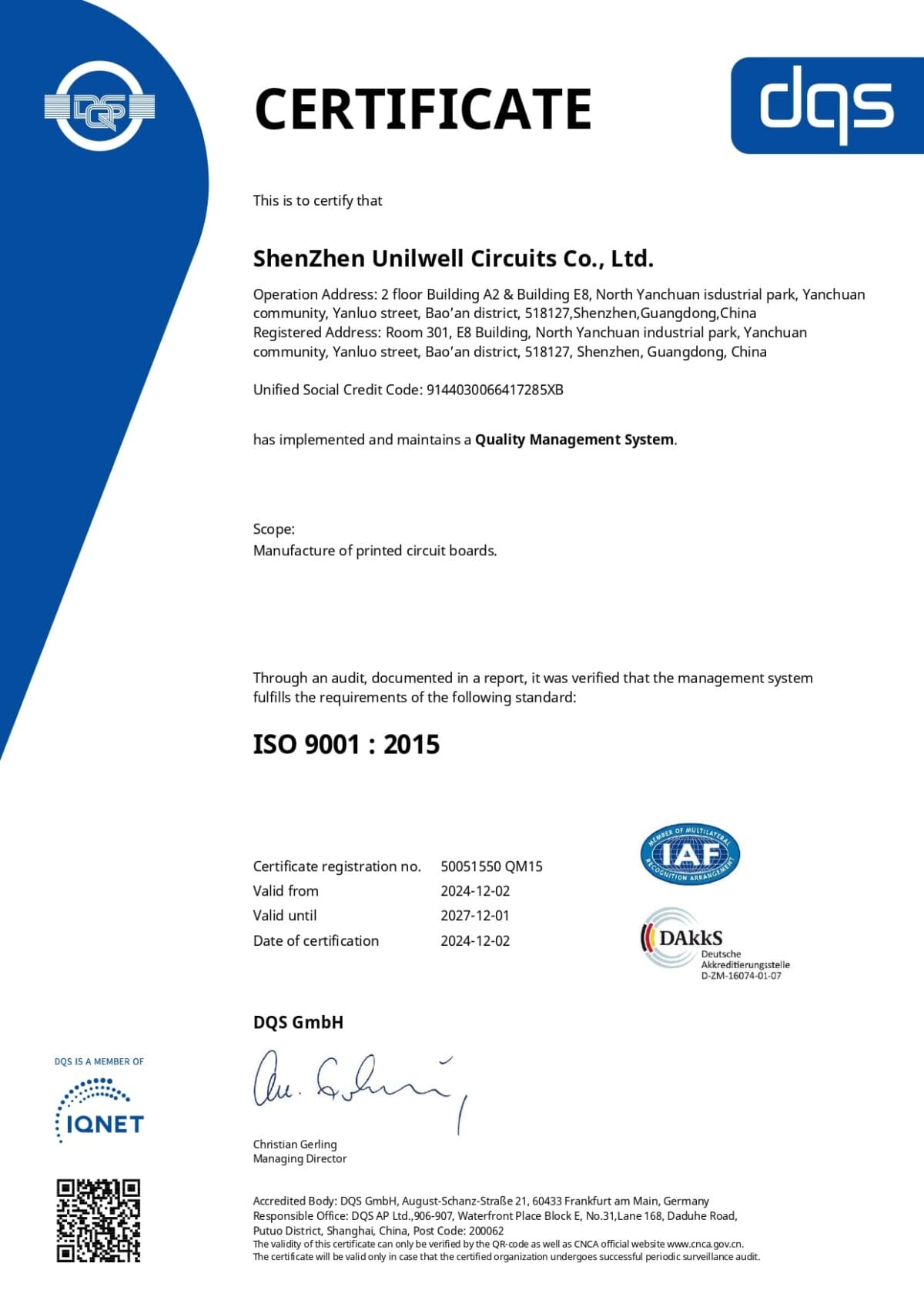
ISO9001 ISO13485
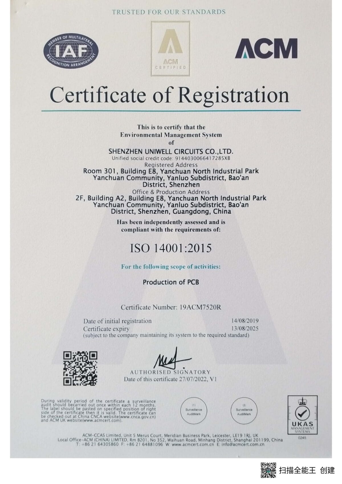
ISO14001

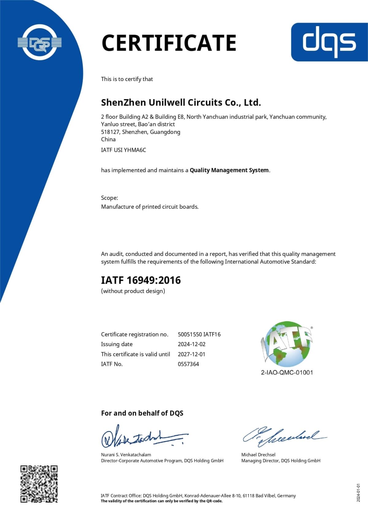
IATF
16949
IPC-A-610H International
Certification

Fully Automated
AOI Inspection

One-Stop Manufacturing & Assembly

Engineering-Driven DFM Support

Advanced Material Options

Certified Manufacturing Capabilities

Heavy Copper & Power Flex Expertise

Rapid Turnaround with Global Reach

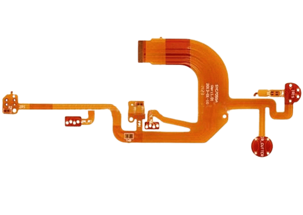
Flexible Polyimide Substrates

DuPont, Pyralux Material Options

Copper Foil

Adhesive Systems

Coverlay Film

1. Cutting
2. Drilling
3. Electroplating
4. Pre-Processing & Dry Film Application
5. Alignment & Exposure
6. Development
7. Graphic Electroplating
8. Etching & Resist Strip
9. Degreasing & Cleaning
10. Surface Treatment
11. Coverlay Application
12. Pressing & Solidification
13. Immersion Nickel (Optional)
14. Silkscreen Printing
15. Electrical Testing
16. Punching
17. Final Inspection & Packaging

Submit Your PCB Design
Upload your Gerber files or use our easy online PCB design tool to create your board layout. Make sure your files are complete and correctly formatted to ensure smooth processing and production accuracy.

Select Your PCB Specifications
Customize your order by choosing the technical specifications—number of layers, board dimensions, thickness, copper weight, solder mask color, surface finish, and more. Our intuitive interface helps you configure everything based on your project’s needs.

Get an Instant Quote
Once your design and specs are in place, you'll receive a transparent, instant quote. Pricing updates in real time as you modify options, so you can adjust your selections to match your budget before placing the order.

Confirm Order & Make Payment
Review your entire order for accuracy, including file previews and selected specs. After confirmation, proceed to secure checkout and choose your preferred payment method. You’ll receive an email confirmation with order details.

Production & Delivery
Your PCB moves into production immediately. We’ll keep you updated throughout the manufacturing process. Once completed, your boards are carefully packed and shipped to your door, with tracking information provided for your convenience.

Aerospace
Flexible PCBs are integrated into navigation systems, radar modules, heads-up displays, temperature sensors, and engine control electronics.
Their ability to tolerate vibration, heat, and continuous flexing makes them suitable for confined airborne assemblies where rigid boards are not viable.

Defense
Military-grade systems use flex circuits in CubeSats, portable targeting devices, missile control boards, and wearable gear.
These builds benefit from reduced connector count, lower profile, and reliable circuit performance under mechanical load and thermal cycling.

Medical Devices
Pacemakers, defibrillators, heart monitors, cochlear implants, hearing aids, and pill cameras use flexible circuit boards to meet strict size, shape, and bend requirements for internal or wearable electronics, enabling reliable circuitry in compact, motion-prone environments.

Consumer Electronics
Used in foldable smartphones, fitness trackers, action cameras, and OLED screen modules, flex PCBs enable tight PCB design inside dynamic housings where mechanical flexibility and signal integrity must coexist.

Automotive Electronics
Infotainment systems, ADAS modules, airbags, lighting systems, and digital dash displays use flexible PCBs to route signals through tight enclosures while tolerating engine vibration and heat.
Their controlled bend radius and material endurance are critical to long-term reliability.

Industrial Equipment
Flex boards are implemented in robotic joints, sensor networks, and compact control systems, delivering durable signal paths in motion-heavy and space-constrained environments.

Telecommunications
Base stations, antennas, portable transceivers, and satellite communications hardware use flexible circuits to manage high-frequency signal paths in ultra-compact RF enclosures.


Hommer Zhao
Founder and Chief Editor – Hommer Zhao
Welcome! I’m Hommer Zhao, the founder and Chief Editor of WellPCB. With years of experience in the PCB industry, I’m committed to making sure our content is both accurate and helpful. We’re proud to serve a growing community of over 4,000 customers worldwide, and our goal is to provide you with the best resources and support. Your satisfaction is our top priority, and we’re here to help you every step of the way!

Jesse Holland
Technical Manager – Jesse Holland
Hi, I’m Jesse Holland, an Engineer and Technical Manager at WellPCB. With years of experience in PCB design and engineering, I’m here to ensure that every project we work on meets the highest technical standards. I lead our team, focusing on precision and innovation, collaborating closely with clients to provide tailored solutions and expert guidance. Whether you’re facing a complex design challenge or need advice on technical aspects, I’m here to ensure your project is a success from start to finish.

Nathan Jensen
Purchasing Manager – Nathan Jensen
Hi, I’m Nathan Jensen, the Purchasing Manager at WellPCB. I’m responsible for sourcing the best materials and components to ensure our products meet the highest quality standards. With my extensive experience in procurement, I work closely with suppliers to secure reliable and cost-effective solutions while maintaining strong relationships to support our operations. I aim to ensure every project runs smoothly by providing the resources needed to deliver on time and to your satisfaction.

Emma
Sales Manager – Emma
Hey, I am Emma, sales manager at WellPCB. I studied electronic science and technology at university and have served customers for PCB and PCB Assembly service for several years.
I enjoy communicating with customers and our technicians to solve problems, and customers always say, "It's great to have you onboard".
It is my pleasure and honour to be helpful. Contact me now, and you'll know.

Bella and Cassiel
Sales Representatives – Bella and Cassiel
We’re Bella and Cassiel, your dedicated sales representatives at WellPCB. With our extensive knowledge of the PCB industry, we’re here to provide exceptional service and support. We take the time to understand your unique needs and are always ready to offer tailored solutions and advice. Whether you need product recommendations, assistance with your orders, or simply have a question, we’re here to ensure your experience is smooth and seamless at every step.

Mandy and Wendy
Sales Representatives – Mandy and Wendy
We’re Mandy and Wendy, your friendly sales representatives at WellPCB. Passionate about helping our customers, we bring a wealth of experience in the PCB industry to provide you with the best solutions and service. We take pride in building strong relationships with our clients, understanding their specific needs, and offering personalised support to ensure their satisfaction. Whether you’re looking for advice, product information, or assistance with any part of your order, we’re here to make your experience as smooth and efficient as possible.
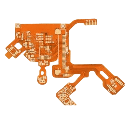
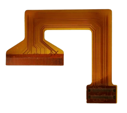
Case Study
A single-layer flex PCB designed for a scanner application, focused on delivering precision signal transmission, mechanical flexibility, and enhanced durability through surface and structural enhancements.
Product Specifications:
- Layer Count: 1 (Single-sided)
- Total Thickness: 0.13 mm
- Material: 1 oz rolled copper with adhesive
- Copper Thickness: 1 oz (35 μm)
- Surface Treatment: Gold Plating
- Min. Line Width / Spacing: 0.1 mm / 0.095 mm
- Reinforcement: FR4 stiffener, 0.5 mm thickness
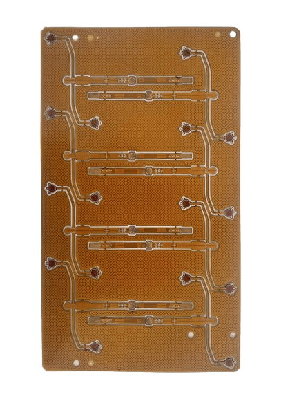
Case Study
This project involves a high-precision multi-layer flexible board developed for use in LCD connectors, focusing on flexibility, signal integrity, and mechanical durability for the flexible connector interface in electronic devices like LCD screens. It includes a multi-layer structure with precise surface finishes and materials to support high-frequency signals while maintaining flexibility and reliability.
Product Specifications:
Material Structure:
- Double-sided adhesive
- Low-loss yellow covering film
- Core buildup: (line copper + glue + high-frequency medium polyimide base material + glue + line copper)
- Outer layers: Low-loss yellow covering film
- Flexibility Requirements: Designed for free bending and winding
- Positional Accuracy (Male Component): ±0.03 mm tolerance
- Thickness: 0.15 mm
- Reinforcement: Front and back reinforced with 0.15 mm steel sheets
- Manufacturing Processes:
- Solder coating
- Plug plating
- Covering layer application
- Film-covered type assembly
- Resistance and welding type shielding torsion
- Surface Treatment: ENIG (Electroless Nickel Immersion Gold, 1 to 2 microinches)
- Minimum Line Width / Spacing: 0.06 mm / 0.09 mm
- Application: Connector components for LCD modules
Case Study
This high-precision ultra-thin flex PCB is engineered for use in advanced medical instruments. The circuit is optimized for biocompatibility, miniaturization, and high signal integrity, meeting the stringent demands of medical environments. It features extremely fine trace dimensions, immersion gold finish, and ultra-thin construction for flexible deployment in compact medical devices.
Product Specifications:
- Application: Medical instruments
- Board Thickness: 0.025 mm (25 μm)
- Surface Treatment: Immersion Gold (Gold Thickness: 1.0 μm)
- Line Width / Spacing: 2 mil / 2 mil (0.05 mm / 0.05 mm)
- Copper Thickness: 8 μm (approx. 1/4 oz)
- Challenge:
- Ultra-Thin Profile (0.025 mm)
- Fine Line Precision (2/2 mil)
- Thin Copper Thickness – 8 μm
- Thicker-than-standard gold layer thickness – 1.0 μm