This tutorial takes you through how you can use Kicad Tutorial in creating, editing, and library linking of PCBs before they are exported to gerbers for fabrications. The tutorial comes in handy for beginners who want to use Kicad. Like Eagle, it will not be easy, but once you get used to it, you will enjoy using it to design your PCB layout.
Step 1: Downloading Kicad Tutorial
The first thing you need to do to get started is to download KiCad. You must contact the latest version of your software, depending on your program.
Once the program has been installed, you need to create a navigation window that will allow you to open the periphery programs, such as PCB layout and schematic capture.
Step 2: Kicad Tutorial—Setting Up the Project
You will have to download the design for KiCad and unzip the files in your local directory. The files that may be needed for this purpose include:
Pro – to help keep track of the structure
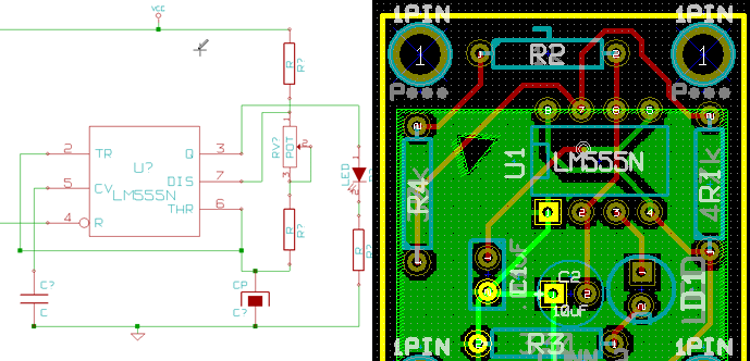
CMP: defines the footprints to be used with schematic components
Kicad PCB layout: they represent the PCB layout
Sch- refers to the schematic
These are the main files that need to be shared on a KiCad design. Also, you may need to share the footprint file.
Notice that KiCad works differently from Eagle and requires that you define the footprint that must go with each component.
Step3: Setting Up the Component Library
It would help if you double-clicked on the Picard Schema. If you get an error, ignore it. If the schematic loads with a question mark, it shows that KiCad is missing the link, and so it may be necessary that you link it to the devices containing the schematic.
Linking your Components to the Libraries
Click on your component libraries and allow for the creation of an open window. The project file has the information regarding where the component library file is located.

Step 4: Adding Components to Your Schematic
If you want to add a device to your schematic, all you need to do is click on add. It opens the component window and allows you to choose a component among the hundreds of features available. The next thing that you need to do is to select the device and press enter. Then place it in your following schematic.
Once the capacitor has been placed, you will notice that it will still be in placement mode. Here, it would help if you hit Esc to return to the normal pointer mode.
Copying the component is easy; just put the mouse at 3.3v and press c to help simulate the device and place it in the required position.
Step 5: Kicad Tutorial—Wiring the Components
It would help if you tried to wire the components together by placing the mouse pointer over the bubbles and pressing W.
Step 6: Annotating the Schematic Components
KiCad helps to auto-annotate your schematic. Here, you should click on annotate the schematic components button, use the default setting, and click to confirm it. Kicad will request that you verify the annotation. Once you confirm, the components will be added.
