PCB Thickness is the technology of PCB is not at a standstill; rather, it has been evolving from level to level and from one stage to another different upgraded stage. As the PCB technology changes, it has been discovered that connecting all the needed components into standoffs to a PCB Thickness is very strenuous. This motivated researchers to find a less labor-intensive procedure, which brought about the single-sided circuit boards.
1.PCB Thickness Technology

The first PCBs were designed simple and with a single-sided board attached to various layers. The boards are made from thin insulating materials, solid and good insulators. As the PCB technology evolved continually, there came the dawn of multiple board connections. This type of connection needs two connectors for each one of the PCBs. One will be for the PCB itself and the other for the rack. As the case may be, the standard PCB thickness of the material that is to be used is 63mils; it means that the corresponding rack connector should also match up to this thickness.
That is how the industry came to the standard PCB thickness specified to be 63mil.
Most times, the majority of the PCBs were not designed with edge connectors.
For instance, single PCBs are made for game products and PC motherboards. There seems to be no reason to use the specified standard PCB thickness of 63mil to make these products, as the 63mil specification was necessary to match up to the thickness of an edge connector. Since the layer counts for the PCBs were increased to match up to the wiring requirements of the more complex circuits, it also produced the circuit boards to have higher layer counts. This jumped from the standard PCB thickness of 63mils to 93mils.
However, with high-temperature materials, Isola’s 370HR can be used in scores of 8, 10, 14, 22, and 39mils, respectively. In other words, the standard PCB thickness depends on the layers of your foil lamination. If the foil lamination is for a four-layer PCB, the standard to be used should be .031+/-10%
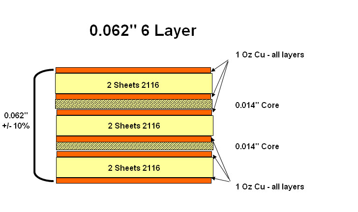
The best standards for a six-layer foil lamination are .062+/-10% or .031+/-10%, respectively.
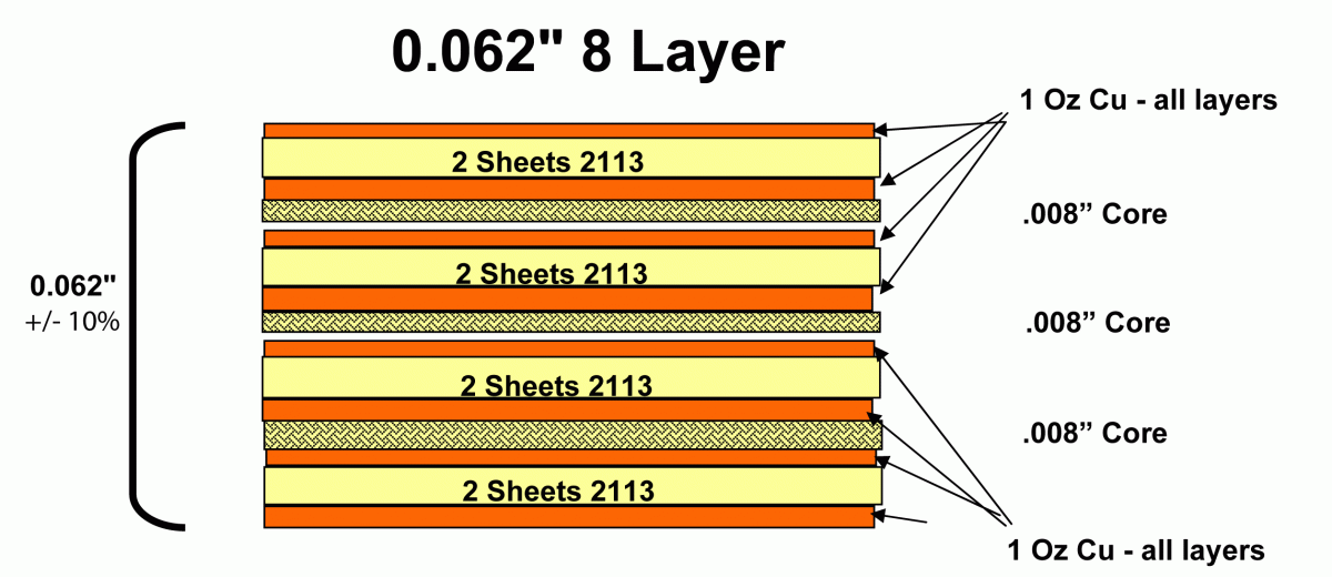
The standard PCB thickness is specified at 0.062, 0.093, and 0.125 inches for 8—and 10-layer boards.
Factors Influencing PCB Thickness
Manufacturers have two main standards for determining standard PCB board thickness. They decide on PCB thickness at the design stage or during manufacturing.
Design Factors Influencing PCB Board Thickness
Choice of PCB Board Material
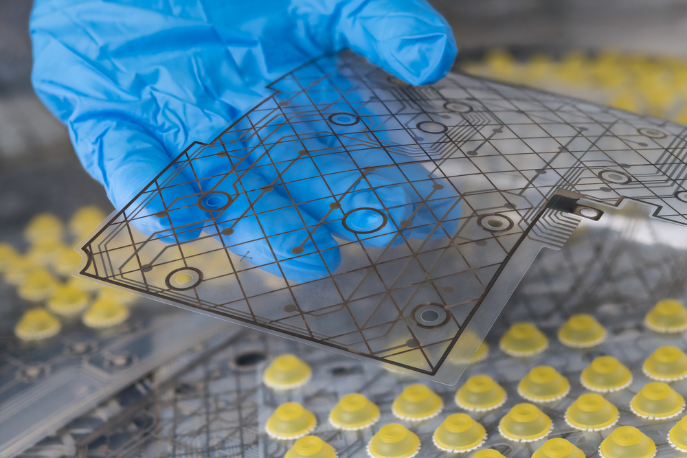
Thin flexible transparent PCB
The board material contributes to the mechanical support, flexibility, and stress-handling capability of the PCB.
For example, FR4 base board material. Your manufacturer might vouch for FR4 for its flexibility, flame handling, and availability.
However, the manufacturer can opt for thick board material — above 3mm — if the purpose of the PCB is high impact or in a structurally stressful application such as automotive.
Thinner lightweight boards, below 1mm, usually apply best in space-sensitive applications such as household electronics or smartphones.
Via Type
As we’ve mentioned, vias in PCBs are passageways that connect layers and enable electrical connectivity.
You’ll need a thick PCB board if you have a buried via that connects at least two layers. Yet, a thinner PCB board is more suitable if you have microvias. Common via sizes range from 0.3-0.6mm.
How Thick is the Copper Layer?
Copper traces influence the carrying capacity in a PCB. Typically, the ideal copper thickness is 1 oz.
If you spread 1 oz of copper to cover one square inch, you end up with 0.0348mm of copper foil thickness.
Increasing the copper layer thickness to account for current carrying capacity means an increase in the PCB board thickness, too.
Application/Operating Environment
While PCBs exist in basically all applications involving electrical connection, the board sizes are not equal in all applications.
For example, low-current applications that have low thermal stability demand thinner PCBs. However, high-impact or harsh environment applications need a thick board that can maintain structure against adverse conditions such as high heat or extreme wind.
How Many Layers Does The PCB Need?
Multilayer PCB
Here’s a fact. A single-layer PCB will most likely be thicker than a multilayer PCB. In fact, the standard PCB thickness for a single-layer PCB is about 1.6mm.
PCBs with 2-6 layers will be thicker. However, a PCB with above 8 layers will pass standard PCB thickness.
Layering affects design in that, you can increase PCB board thickness instead of using more layers. It reduces the number of layers but still meets thickness requirements according to the design.
Signal Types
PCBs have high-power signals or complex signals.
Typically, high-power signals do well in thicker PCB boards. This is because the high-power signals need thick copper thickness with wide traces. You will find high-power signals in low-power applications and environments.
However, complex signals are more common in high-density boards. HDI(High-Density Interconnect) boards use thinner material for high performance. Furthermore, they have microvias and thinner traces.
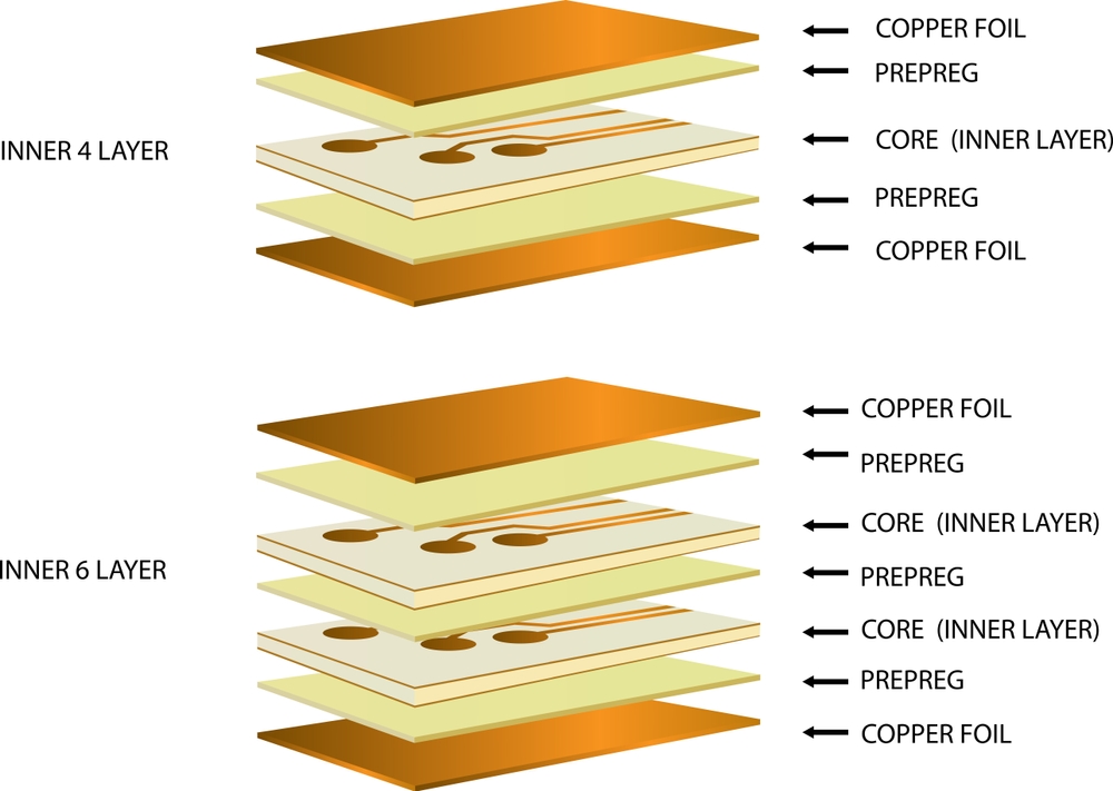
Insulation Layer Thickness
The insulation layer or prepreg exists between the core and copper foil or between two cores in a PCB.
It acts as insulation, a binder between cores, or a short circuit protector in multilayer boards.
Prepreg type depends on how much prepreg a manufacturer uses. High Resin Prepreg(HR) thickens the PCB. However, the manufacturer can use medium resin(MR) or standard resin(SR) to reduce PCB thickness and cut costs.
It ranges between 0.0508mm and 0.1194mm.
Manufacturing Factors Influencing PCB Board Thickness
PCB thickness decisions aren’t only on the design level. Manufacturing processes and tools can determine the thickness of the PCB.
Method of Depanelization
A PCB manufacturer can stack several boards into a panel. This panel or block is then detached or depanelized to form individual boards.
Depanelization has several methods that affect the PCB thickness. Some common methods include V-Score shearing, routing, and manual breaking,
Scoring, as a depaneling method, is handy when dealing with thick PCB boards. Thinner boards go through routing for the breakaway tabs.
Drilling equipment
There is a standard drilling aspect that manufacturers stick to. The 7:1 drill hole depth to drill hole diameter aspect ratio works for most PCBs. Exceeding this standard ratio and using a custom ratio increases costs and is subject to an agreement during the design phase.
Thicker boards will most likely require a custom ratio that calls for larger-diameter drill holes.
Copper thickness
As much as copper thickness is a design factor in PCB thickness, it also affects manufacturing. Copper traces must undergo etching and plating, key aspects during manufacturing.
Thicker copper layers affect these processes compared to thinner copper layers. The choice of copper thickness affects the manufacturing process and the overall thickness of the PCB.
Layers
Increasing PCB layers can make manufacturing to a standard thickness very challenging. And since not every manufacturer can meet these custom needs, you must find one with the right tools and expertise.
Like the drilling equipment, you also need to bring the layer count discussion up at the design phase.
FAQs
Q: What is the standard thickness of a PCB?
The industry standard thickness of PCBs is about 1.6mm(0.063”)
This standard thickness includes copper layers and the silk screen.
However, the standard thickness for a 2-layer PCBs can start from 0.180mm, while the standard thickness for a 4-layer PCB is between 1 and 5mm.
Since standard PCBs go in portable devices, the standard thickness meets mechanical strength, weight and portability standards.
Additionally, it is easy to manufacture 1.6mm thick PCBs using standard equipment and processes.
Still, there are other ‘standard’ PCB thickness measurements. Measurements such as 2.36mm and 3.17mm are common but subject to agreement between the client and the manufacturer.
Q: How does PCB thickness affect thermal performance?
Thick PCBs have higher heat dissipation capacity, making them ideal for high-performance applications.
Also, you need a thicker PCB to include additional components that manage heat, such as heat sinks. The increased surface area of thicker PCBs provides enough space to distribute heat evenly and maintain safety standards.
Q: How does this affect signal integrity?
High-speed signals are more susceptible to distortion in thinner PCBs. Therefore, you need boards with better impedance control to tone down signal reflections and crosstalk.
Thick PCBs offer better impedance control, making them preferable for more accurate digital transmission.
