It is required that vias and traces should conduct electricity. However, it is not in order if they conduct electricity in places or areas not designed to conduct electricity. Can vias and traces conduct electricity on a PCB surface? The short answer is yes and no. We must go back to the basics of what vias and what traces are for the long answer.
1. What Is Vias
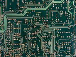
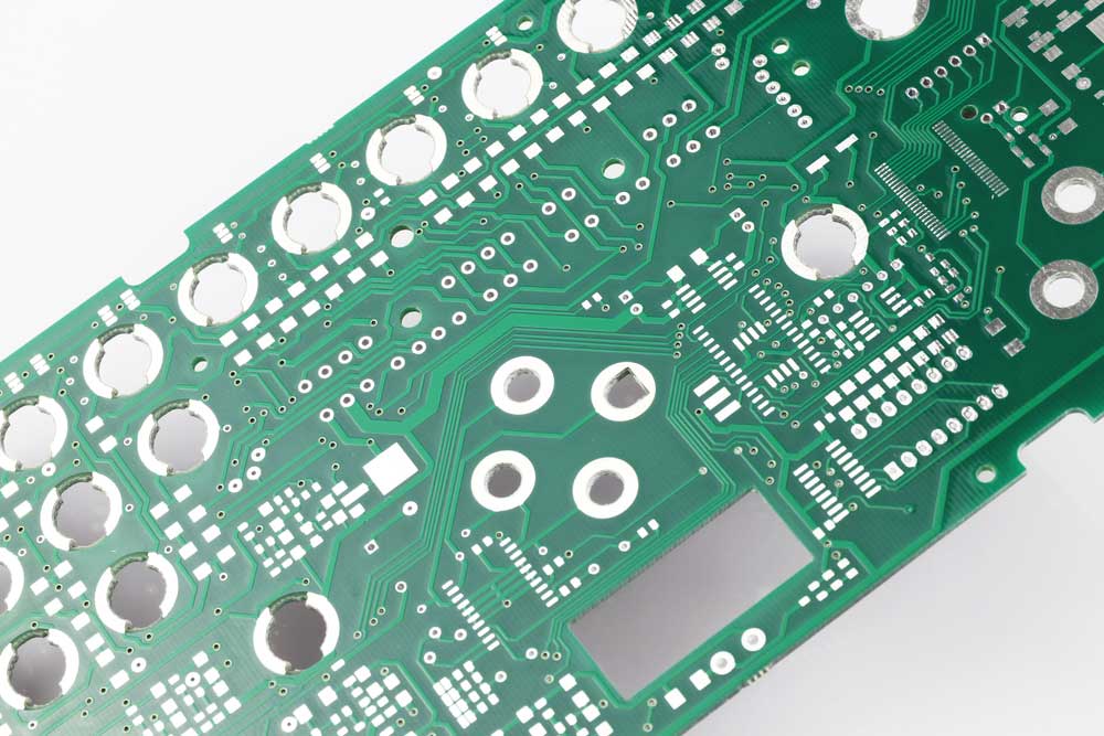
Vias are basically conducting holes on the PCB. They electrically connect one PCB Layer with another, say, connecting the top PCB layer with the bottom PCB layer. Vias could also connect layers in between. On the other hand, Traces are meant to conduct electricity from one PCB component or PCB pad to the other. In other words, PCB traces act as conducting copper wires on the PCB.
2. What to Consider When Designing Vias
When designing a PCB, one has to consider a couple of parameters. One of the most important considerations is the size and position of vias and traces. When using PCB Design software, it is easy to ensure that these conditions are well met. If these conditions are not met, vias and traces on the PCB surface could conduct electricity. Cause a short circuit on areas or sections that are not anticipated.
One of the basic measures that ensure that a PCB will not conduct electricity on a PCB surface is to apply a solder mask. Obviously, if a PCB is not covered with a solder mask, it will definitely conduct electricity when a metallic material rests or touches its surface. However, a solder mask cannot be relied upon to prevent vias and traces from conducting electricity on the PCB surface. A casing should cover the PCB to prevent objects that could cause or facilitate vias and traces to form a short circuit.
The PCB design rule check is helpful in making sure that it raises errors when the design goes outside the recommended specification. In addition to these alerts, it is advisable to plan your PCB in such a way that it is free from potential electrical flaws. For example, you intend to solder a USB port or a memory card slot on a PCB. It is advisable that you avoid putting the vias or traces below these components unless it is very necessary. This is because of the friction and the mechanical movements involved when attaching and detaching these memory sticks.