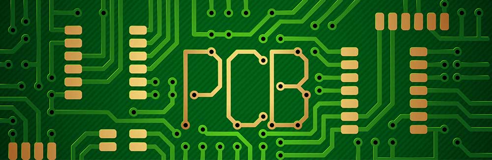
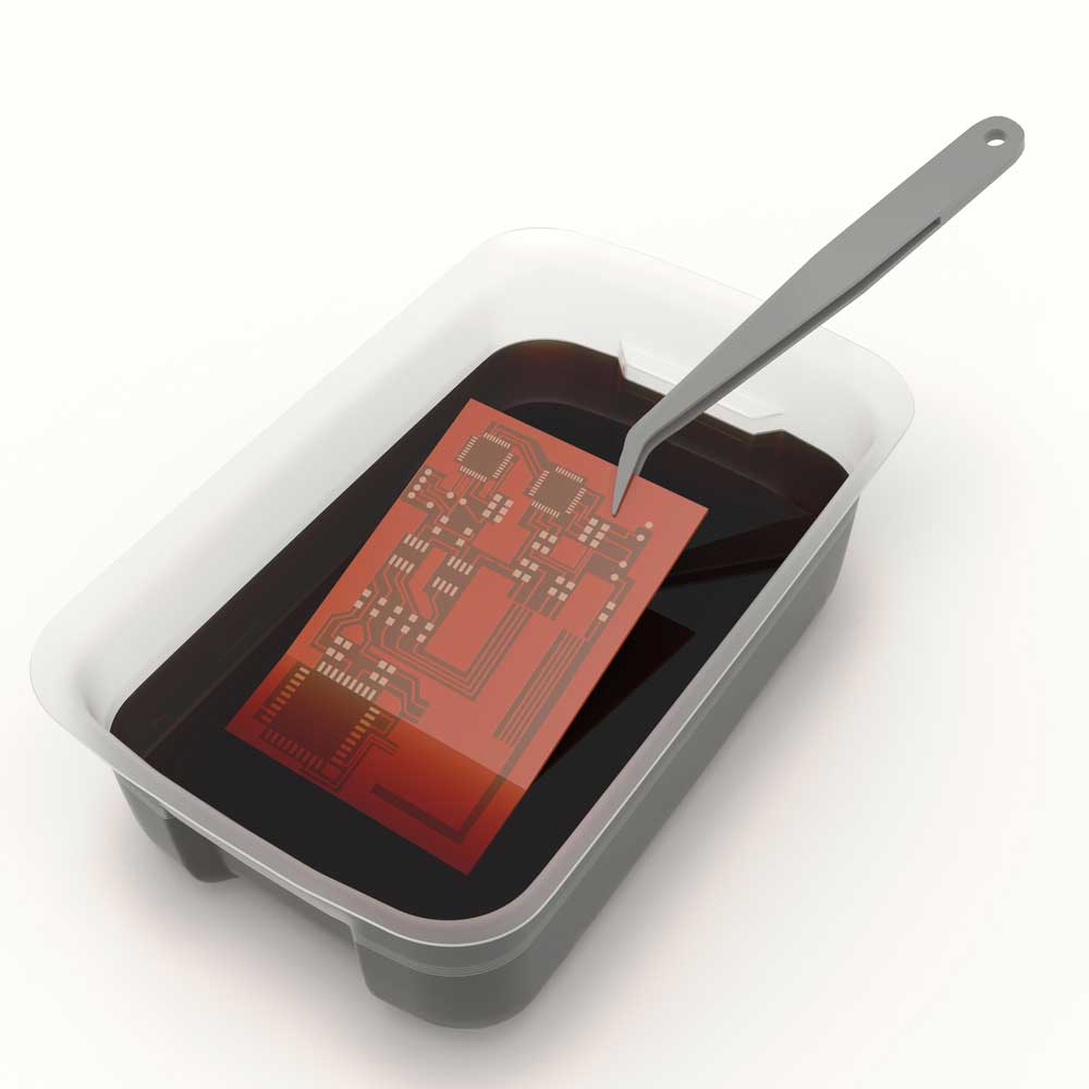
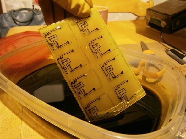
Etching PCBs is a “subtractive” method used to produce printed circuit boards: acid is used to remove unwanted copper from a prefabricated laminate. This is done by applying a temporary mask that protects parts of the laminate from the acid and leaves the desired copper layer untouched.
You can etch a PCB by yourself, in a labor even at home, through a simple and inexpensive production process. The PCB etching process is therefore effective for a small workshop.
1. There are, however, some issues to consider:
1.1. There is a risk of injuries due to the chemicals involved.
1.2. The quality of the results depends on several factors which you won’t be able to master completely the first time. This can be somewhat compensated by using good machinery.
1.3. There is the problem of waste disposal. Toxic chemicals require a proper disposal service.
To learn how to etch a PCB, make sure that your Fritzing PCB design is complete and exported as an etchable PDF or SVG, then follow these instructions.
2. Instructions of Etching PCBs
Anyway,
Second, Preparing the Board and the Toner Transfer because you have to transfer the toner on the magazine paper to the copper board. Make sure your copper board is as clean as possible and don’t handle it too much and also make sure your iron is as hot as possible but with the steam function turned off.
Thirdly, you can start etching.
3. The things you need to pay attention to are:
3.1. The choice of Etching PCBs solution
Sulfuric acid-hydrogen peroxide etching solution: It can be used for micro-etching before the plating. It has been used in PCB etching in recent years. It is characterized by non – Corrosion of tin-lead alloy; the solution is straightforward, the only product after the etching of copper sulfate. The etching solution can be recycled and recovered to obtain high purity copper sulfate crystal. Therefore, it can reduce wastewater emissions and environmental pollution. It is a promising etching solution.
Etching mechanism: H2O2→H2O+(O)
Cu+(O) →CuO
CuO+H2SO4→H2O+CuSO4
Cu+H2O2+H2SO4→2H2O+CuSO4
hydrochloric acid-hydrogen peroxide etching solution: Simple operation, fast, low-cost ,especially suitable for producing large area PCBs
Acid-hydrogen peroxide etching solution Typical processes for etching are as follows:
3. 2. Photolithography was used to coat the conductor circuit on the circuit board, and many of the steps in the process used plasma technology.
First, the metal layer’s entire surface needs to be coated, and the photoresist layer is coated. The photoresist layer is exposed and developed. Meanwhile, the structure of the subsequent conductor circuit is still covered by photoresist.
Next, remove the metal layer from the uncovered area by Reactive Ion Etching (RIE).
Then, Remove Toner: the photoresist on the conductor circuit is removed by plasma etching in an oxygen plasma
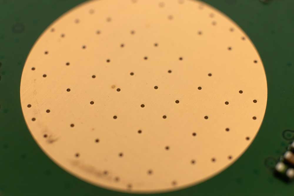
4. Drilling & Tinning
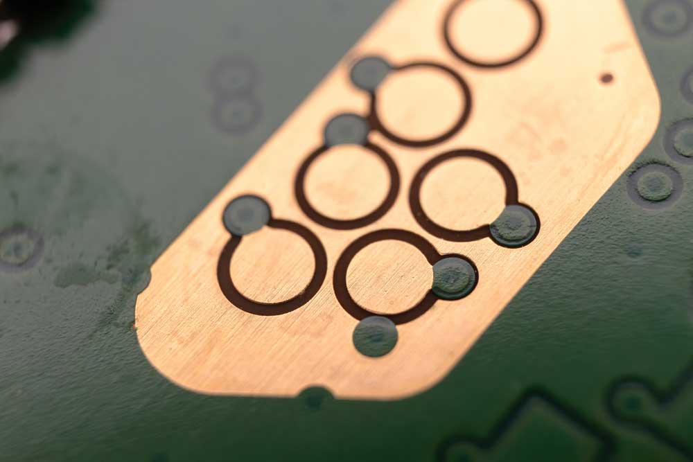
You’ll now need to drill all the holes in the board. I suggest getting a drill press accessory for your Dremel to do this, although I’m sure you could do it fine with a steady hand and a bit of patience.
I drilled all the LED/cable holes with a 0.8mm bit and the screw holes with the M3 bit.
Then, an etching PCBs is basically finished.