PCB is used for permanently soldered circuits like small-scale and large-scale electronic accessories and gadgets in different industries. Marketable courses or gadgets are always made with PCBs.
The PCB electronics component is an electrical or electronic device, such as an inductor, resistor, capacitor, and IC, that processes the input electrical signal.
Each component has a unique symbol maintained throughout, from schematic drawing to PCB layout. The characters are made for electrical PCB assembly.
The marks made for PCB layout are called component footprints that define the component’s to-the-scale shape and soldering point. The component symbols and footprint may be of the same or different conditions.
PCB Electronics–Content
The PCBs have conductive thin copper tracks on one side in single-layer PCBs, on both sides in double-layer boards, and multiple layers embedded within the outermost two layers of the board.
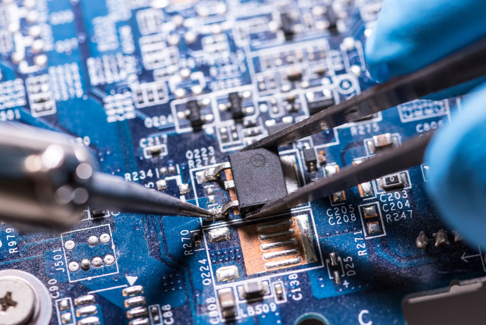
The tracks, generally covered with a masked coating, propagate signals from one end to the other. Typically, for a single-layer, double-layer, and multilayer PCB, the through-hole components are mounted on one side and soldered on the other side of the PCB.
The SMT components are mounted and soldered on the same side of the PCB. The component density over the multilayer PCBs is much higher than the single and double-layer PCBs.
Generally, the PCB electronics components are categorized but not limited to the following types.
Resistor: general-purpose fixed, single or multiturn variable, slider, temperature-dependent, etc.
Switches: Push to ON, Push to off, rotary, toggle, limit, etc.
Inductors: power supply inductors, high-frequency RF inductors, filter inductors, etc.
Capacitor: polar and non-polar capacitors, high frequency, power supply, etc.
Diode: General purpose power supply rectifier type, Zener, Schottky, transient voltage suppressor,r, etc
Transistor: NPN and PNP BJT, N-channel and P-channel FETs, UJTs, etc
ICs: Analog ICs like operational amplifiers and sensors, digital ICs like gates, microprocessors, comparators, memories, FPGAs, DSPs, etc. From the PCB perspective, each has its unique symbol and pin names for drawing clarity.
Figure 1 shows the different resistor and capacitor footprints; figure 2 shows the 32-pin SMD IC schematic symbol and print, and figure 3 shows the placement of the SMD package IC for soldering.
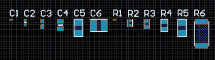
1: Different sizes and shapes of capacitor and resistor footprints.
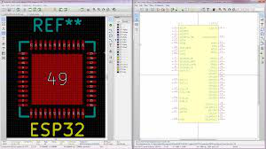
2: IC footprint and schematic symbol
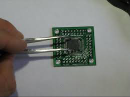

3: 8-pin SOIC footprint 3D PCB footprint model and soldering on PCB
