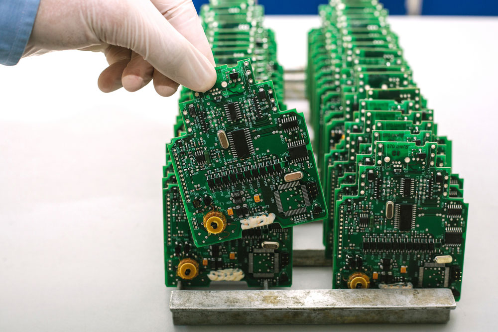
Printed circuit boards (PCBs) are the backbone of electronics and are widely applied in manufacturing computational electronics, including various digital devices.
The purpose of PCBs is to direct the electrical current to where it is designed to flow.
PCBs produce electrical current through a network of copper pathways.
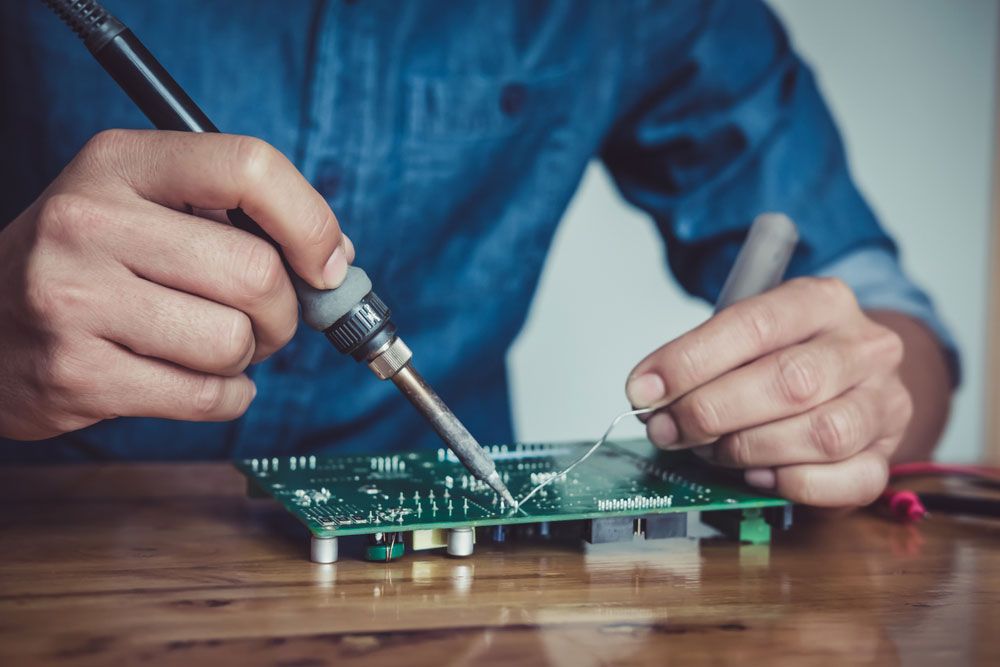
So how are the PCBs manufactured?
PCB Manufacturing Process–Content
PCB Manufacturing is a complex process that starts with the design of the PCBs.
Designers use programs such as extended Gerber to create a layout. The software encodes the required information, including the components notation and copper tracking layers.
The PCB design is then forwarded to the manufacturing company. Following a DMF check, the PCB schematic is printed on a film using a plotter.
The movies are then used to image the PCBs. Once the film is ready, the manufacturer prepares to make the actual PCB which comprises a laminate board.
This body will receive the copper that will structure the PCB.
The next thing is to put a layer of a photo-sensitive film called photoresists, which are just reactive chemicals that harden when exposed to ultraviolet light.
The movie fits and holds the pins on the laminate panel. Any unwanted copper is then removed using an alkaline solution.
The hardened resist used to protect the copper is then washed off using another solvent. The layers are then aligned by punching holes using an optical punch machine.
The formed layers are then fused, and a thin copper foil is used to cover them before they are sandwiched together.
Holes are then drilled into the board. The holes will be used for copper linking.
They are small holes with a diameter of about 100 microns.
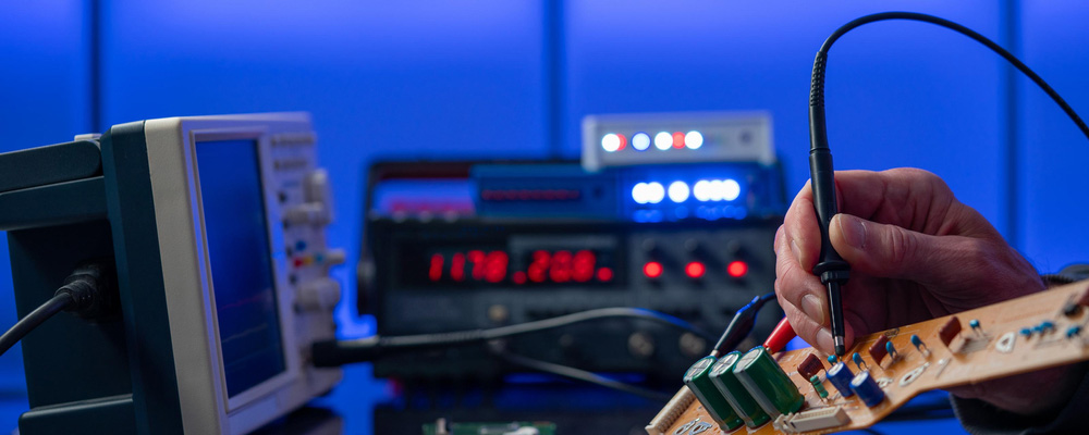
After drilling the holes, plating is done to fuse the different layers. This is done using a chemical deposition. A layer of photoresist is then applied to the panel. The board will then be passed through an oven to cure the solder mask. It is then chemically plated with gold and silver before electrical tests are performed to confirm its functionality.
