On Diptrace Study Guide, Recently we made a return visit question: Which PCB design software is the customer using. Click here to learn about our collection of design software.
Diptrace received 50% of voting support. What reason did some designers choose this?
This will be the starting point for writing this guide.
Diptrace is a circuit design software that maximizes the productivity of circuit design. Diptrace allows you to quickly and efficiently create complex circuits and gives you the advantage of rapidly checking for errors.
By reading this guide, I am confident that you will have a deeper understanding of Diptrace and become a master of Diptrace.
What is Diptrace?
Diptrace is an ECA/CAD software to build schematic design and the printed circuit board. You can quickly create any schematics and then change it to the other formats, i.ne., PCB.
Diptrace allows the user to use primary and flexible features like 3D modeling, high-speed shape-based routing, and extensive import/export capabilities.
While switching from one format to another format, it also assembles the electrical components. It offers multi-sheet and multi-level hierarchal circuits Diptrace has four modules. Its functionality details are described in the following sections.
You can also check out a detailed guide about Diptrace software.
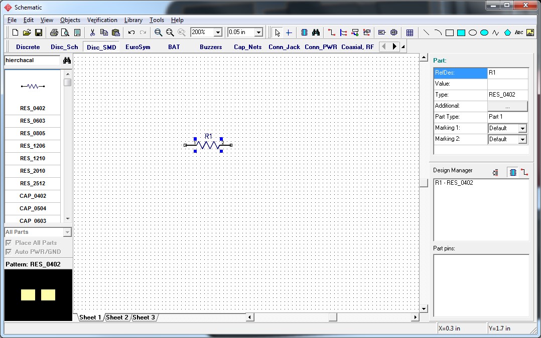
1.1 Schematic capture
The schematic capture section allows the user to connect the pins visually, without wires, logically or using the net ports embedded in the circuit board. It can convert schematics to PCB, annotate easily, and be imported/exported from other CAD/EDA software and formats.
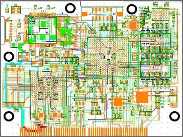
That will happen with the advanced cross-module management function which is present in the Diptrace. A simple figure of a schematic design is shown below.
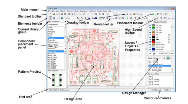
1.2 Diptrace Study Guide—PCB Layout
The following module is the PCB layout. It uses a high-quality board-level design tool that is helpful for intelligent placement, routing tool, shape base auto-router, copying blocks, and creative projects.
Manufacturing of PCBs, there are high chances of layout failures, which can go a long way into negatively affecting the final product’s functionality. There are several PCB layouts that are a high-level engineering tool for board design featuring intelligent manual routing of high-speed and differential signals.
The verification feature is one of the essential characteristics from which you can quickly check the accuracy of the complicated project accuracy using high-speed signals.
It contains one more helpful tool named real-time DRC that is used to fix errors and enhance the quality of the project until it is compiled the project.
1.3 Diptrace Library Creation
Another introductory module is Library creation, divided into two significant parts, i.ne., component and pattern editor. Looking to the component editor helps the user manage libraries and create single or multi-bit components by selecting an integrated template.
Using the pattern editor, you can draw the pattern with numerous shapes, pads, holes, and dimensions. It contains circle, square, matrix, rectangle, and zig-zag templates.
You can also create the non-custom patterns using the DXF import makes creating complex layouts easier. The user can also create complex components, and design’s using different features like bulk pins- naming, pad numbering, and editing.
1.4 Diptrace Study Guide—3D Modeling
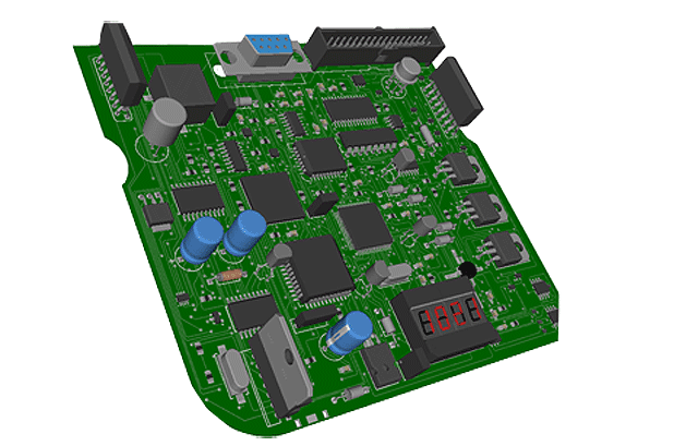
The necessary and helpful module is 3D modeling used to show the circuit board components in 3D view. That allows the board to rotate at axes, zoom in and out, change the color of the board, copper area, solder mask, silkscreen, and background.
The significant advantage of 3D modeling is it works on all stages of the design. The fundamental purpose of this module is to give the user a path to view the circuit board from any angle or any side to check the maximum errors.
1.5 Diptrace Study Guide—Component Editor
It is used to manage component libraries and help to create multi-part components. The engineer can use it to select a template and its dimensions set up. The model defines the electrical pin parameters and attaches patterns with 3D models.
Diptrace can then be used to import libraries from various EDA formats. It can be used to create non-standard patterns as well as creating complex layouts. All that one needs to do is to select the template and enter essential parameters.
1.6 Diptrace Study Guide—Pattern Editor
It is used to create patterns of different dimensions and shapes. It can also draw holes, lines, pads, circles, squares,s, and sizes. Pattern editor helps the engineers to draw zigzag and rectangles, templates.
Selecting an appropriate pattern helps the engineers to draw silkscreen and enter a couple of relevant parameters, including creating non-standard designs.
Diptrace Tutorial(step by step)
2.1 How to create the schematic in Diptrace
This Diptrace software is relatively easy to use and very user-friendly. Schematics in Diptrace is a module for creating and editing electrical designs. Before going to the creation of the schematics, you should know about the schematics basics.
The user can quickly draw any circuit diagram and check that whether this is correct or not.
So creating a schematic follows the several steps in Diptrace. From which some of the important ones are listed below:
First, you have to set the sheet size and select the template of the design. For this, go to the “file/titles and sheet setup.”
You can also change the units of broader widths and different measurements.
I. You should make sure that the grid must be ON because it helps to place the components accurately. To start the grid, press the F11 hotkey directly. Otherwise, go to the “file/ grid size” from here; you can customize the grid as per your requirement. Start the software and on the grid (if it is not on) through an F11 hotkey.
Ctrl+plus sign may also change the size of the grid, increases the size, and Ctrl+negative character decreases the grid size, and the same procedure is followed in the PCB manufacturer, then the process is more hectic. They will design the PCB layout.
I. You can also change the color and the graphics mode of the sheet through “file/ color or graphics modes.”
II. Diptracne contains two types of libraries,i.e., libraries and all libraries. Select the libraries from these two libraries points or add more libraries in this.
III. Then, you have to place the components by searching in the libraries. If the details are multi-part, you will recognize them one by one by the drag-drop method (drag with a right-click and drop with a left-click).
IV. After placing the components, the primary task is to make the connections. There are two methods of doing this nets and buses.
Nets support several methods to connect the pins of the components.
- Direct connection easily connect the pins easily. Choose the wire option from the toolbar and click on the first pin and connect it with the next pin.
- Connecting with the net ports helps to connect the pins more efficiently as it provides GND and POWER automatically.
- Connection without wires this feature is helpful when the density of the circuit is very high then you don’t need to connect the pins through wires.
- Global nets connection are useful where hierarchy are united. What you have to do is go to the web properties and choose the global net and start using.
- Connection with buses is related where there are several small circuits with similar functionality are present in a bus. So this is easy to get separately connected the nets through a pin in a bus. Bus connectors are also used for connecting the different buses.
V. Diptrace provides you with different functionality and provides you with the workplace you needed like. If the circuit diagram is small, then one sheet is more than enough, but if the circuit is large, then what to do? Go to the “edit/add sheet” from the main menu or right-click on the tab and insert from the submenu.
VI. Moreover, after that, you can set the properties of the component and save the schematics at any of the folders of your computer.
Once you build the circuit diagram, you can change it to different PCB formats and others. First, we need to discuss how you can quickly create the layout.
2.2 How to create layout and design PCB
User interface PCB design is similar to the other applications windows. PCB layout allows the user to edit and create printed circuit boards. Switching is needed where you have to make complex circuits, and it is challenging to develop courses directly in PCB layout, so this switching is beneficial.
Switching from schematics to layout follows several steps, which are given below:
I. Select the circuit design and go to the file, and select convert PCB, or you can press Ctrl+B. In this way, you can change the schematics to the PCB layout.
II. Sometimes, you need to renew your schematics for this. Go to the “file /renew layouts from the schematics” from the main menu of the PCB layout. It has several update options like:
- By components
- RefDes
- By related schematics
2.3 Diptrace Study Guide—Designing of PCB
I. Launch the PCB layout. The design area is blank until you open a file, or you can also open your schematic file.
II. After launching the PCB set the place board outline and the coordinates as per the expected PCB size.
III. Then, move the circuit diagram into that area by drag-drop method.
IV. The object can easily be rotated by pressing the hotkey R.
V. Select the mounting hole from the toolbar and place it, open the properties and set the X & Y co-ordinates
VI. This will also be done with DXF import. When the shape’s contour is very complex, you can easily convert it to the border outline.
VII. You can add the text from the toolbar
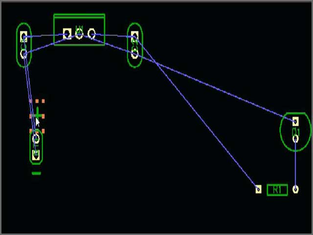
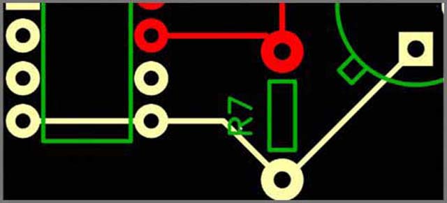
VIII. Selected the manual routing option and made a path of routing.
IX. Select the copper pours and adds the properties as you want. Copper pours are used to fill the spaces into the board. It is usually used to connect the pads to the GND and POWER on the inner plane layers of the multi-plane layers. Add the features of the copper pour.
X. After the copper pour, you need to add the post-routing features.
• Pattern marking
• RefDes renumbering
XI. After all that, add dimensions; through this, you can resize the PCB board easily.
XII. Panelizing is an essential tool. With the help of this command, you can quickly reduce the cost of the PCB board.
This will be done with two methods:
• Several boards are united into one panel
• Copy/paste method
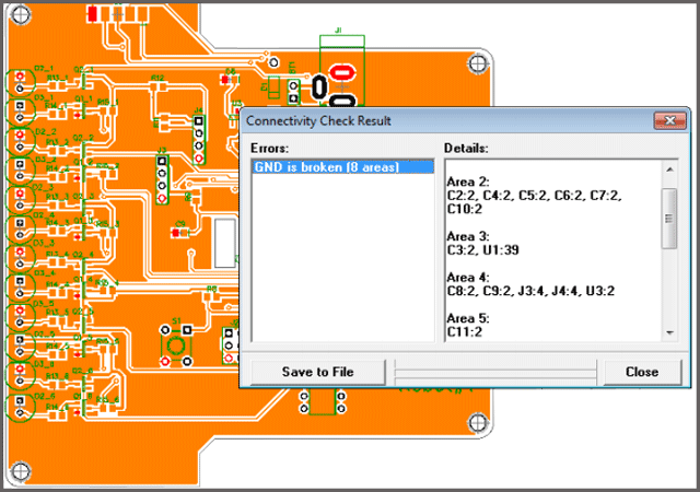
XVIII. You can check the errors of the circuit, go to the verification, and select electrical rule check (ERC); this step indicates that whether the error is found or not.
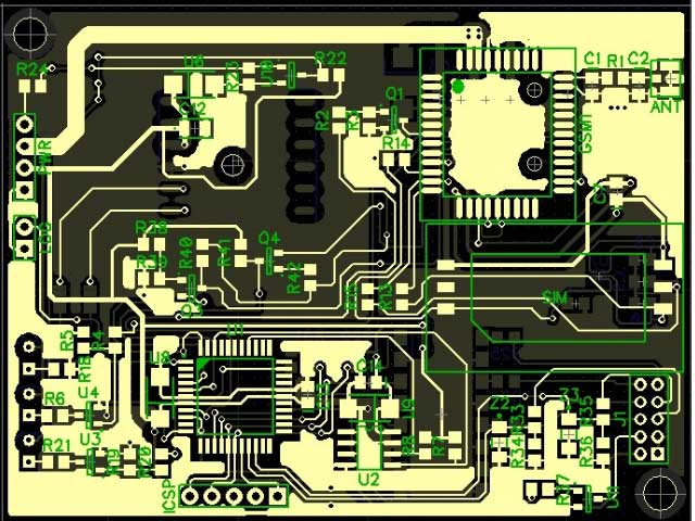
LAYOUT:
PCB LAYOUT:
IF THE ERROR WILL OCCUR
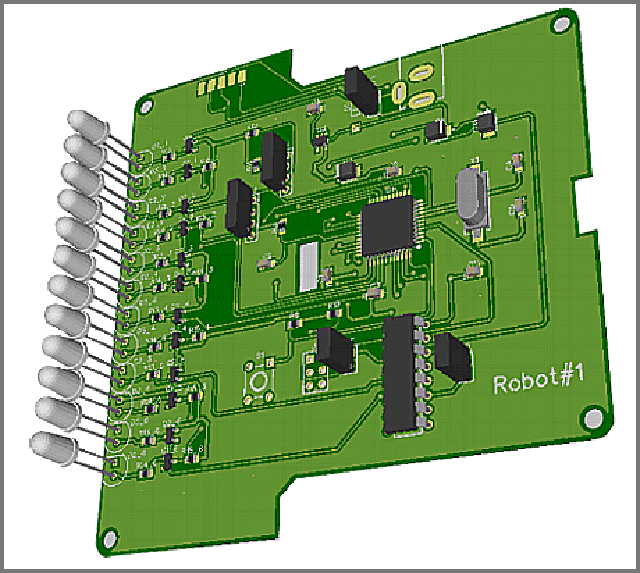
3D PREVIEW OF THE DESIGN
“GO TO THE TOOLS/3D PREVIEW/3D VISUALIZATION.”
A complete video tutorial is available for you on the link below
https://www.youtube.com/watch?v=McOu1DAu9TA
Diptrace Generate & Diptrace Download
3.1 Diptrace Study Guide—Diptrace Download
Diptrace has many versions that are available for free download.
The latest version, 3.1, is available for download. Diptrace required win7/win8 (both 32 bit and 64 bit), Linux or wine MacOS x leopard or newer or OS, Windows 2000/XP with 500Mb free space in the hard drive, 256Mb RAM, and 1024×768 monitor resolution with 8Mb video RAM. Very few changes are present, although this is straightforward software to use and also very user-friendly. One may quickly learn the software in days.
3.2 Transfer Other File Formats to Diptrace
Yes, it can transfer the PCB files to the other formats, i.ne., the user can easily transfer the file into five given formats:
►PCB design(*.dip)
►schematics(*.dch)
►Pattern library(*.lib)
►Component library(*.eli)
►PCB design(*.rul)
Go to the File option and select export the formats you want, and the PCB file will automatically convert into that file, and then you can easily change the setting as per your requirement. From all of the above formats, you can change the PCB file as your requirement.
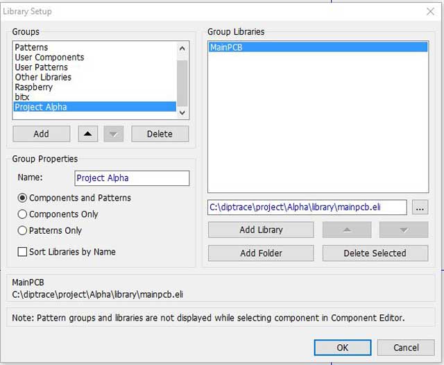
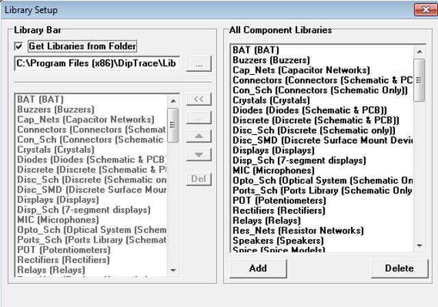
Diptrace Libraries
Diptrace has two important libraries which control the pattern and components of different functions, ne.g., libraries and all libraries. Libraries contain essential selective parts of the libraries, but all libraries include libraries, i.ne., user library, import/export library, etc.
• You can import and export the components of your own choice
• You can quickly add libraries of your own. For this, go to the library from the toolbar, select library setup, choose user component, press the add library button, and name the library what you want.
• Similarly, many libraries are present in the software. Only you have to add the library and start the design in the design area.
Diptrace VS Other Design Software
5.1 Diptrace Study Guide—Diptrace vs. eagle
| Serial number | EAGLE | DIPTRACE |
| 1. | Less intuitive | More intuitive & easy to use |
| 2. | It takes more time to create the circuit because of complexity, and also libraries are a bit hard to manage | It is simple and consumes less time to build a course and libraries are manageable |
| 3. | The 3D view is more realistic. | The 3D view is less realistic. |
| 4. | Sheets are challenging to move, but you can move the component select component right-click move | You can quickly move the sheet by holding the right mouse and components by holding down the left mouse |
| 5. | To view, the libraries go to edit | Libraries appear on the upper side of the schematic editor. |
| 6. | You can delete the components one by one, not by selecting all parts. | Quickly remove the unwanted components by just selecting and press the delete button |
| 7. | Inbuilt LT spice simulator | No built-in simulator |
5.2 Diptrace vs. Kicad
| Serial number | KICAD | DIPTRACE |
| 1. | Many shortcuts are available. | Decent libraries are present. |
| 2. | Many decent libraries are available. | Decent design layout rules are also current. |
| 3. | It supports the program, and a couple of workers work simultaneously on that, but it is unpredictable how long it will keep it. | There are no so many shortcuts are present. |
| 4. | It is complex many times. | It is simple to use |
| 5. | Sometimes the non-intuitive way to do things | More intuitive to do things |
| 6. | Place junction only works when the wire touches a pin at the connection point. Otherwise, it will not work | any interactive routing like push shove, real-time DRC implemented so far |
Diptrace Study Guide–Other features
•High-speed shape-based auto-router
•Advanced verifications with real-time DRC
•Real-time 3D PCB preview
It allows for export features and real-time 3D review. Displays models of the manufactured printed board and the installed components. Will enable the engineer to rotate the board, zoom it in and out whenever they want.
It also allows them to change colors, including the background.
Note that the Diptrace free version is available and comes with all the functionality you will get in the complete package. Perhaps the only limitation you will have to fathom is that it is limited to 300 pins but can be used to create a four-layer board with full ground planes and full power.
•Export of PCB to Step 3D file format
•ODB++ and Gerber (including Gerber X2) manufacturing outputs
Many other features are used to control the different functions, i.ne., component searching, checking connectivity, checking ERC (electrical rule checks), and many other features.
These features are compatible because they can exist in either of the states it means that the file can exist in PCB layout or as Gerber or any other layout feature.
This software is free for download. You can quickly build straightforward projects on this free version, but if you have to develop any complex tasks, you have to purchase an unlimited version price of $895.
That includes all other features and other facilities.
Diptrace Study Guide–Diptrace User Comments
Pros of Diptrace:
* I use Diptrace. I had been using PADS at my job and was let go. When I started consulting, I had to have something I could afford. You can get a two-signal layer package that can do four-layer boards as long as two layers are planes only. It included a large selection of AVR library parts – just lacking the very new stuff. Over 50,000 library parts included.
*It does have an auto-router and auto-placement tool, but I can’t comment on how that works since I haven’t used it yet. Like any auto-router, before you press route, you have to learn how to set the rules. It output great Gerber files, and I had boards made at Myron PCB that worked just great.
*DipTrace allows for a lovely Bill of Material output. You can define your fields and even assign a link to the datasheet on the internet. Right-click on the part and select the datasheet from the popup, and your browser opens with the datasheet. It can panel analyze and import/export Gerber, DXF, netlists of all sorts, and other package formats, including pick and place files.
*You can change the schematic and update to the PCB and change the PCB and update the schematic. The verification features allow you to check the board to the schematic and design rules to ensure there are no errors before sending out your CAM files.
Cons of Diptrace:
*It lacks in the connector libraries. But, with so many options, it’s no wonder. If you use D-Subs, and 0.1″ pin headers a lot, you’re covered. Searching for an SMT 6 volt TVS is difficult unless you know the part number.
Diptrace Study Guide–Conclusion
From the previous discussion, it is clear that Diptrace is straightforward and user-friendly software. They have many different functions and parts to entertain every kind of user.
Diptrace is an easy-to-use software and saves the time of the user and money; very complicated and challenging circuits are made very quickly and easily. You can also check whether the schematic is correct or not?
Similarly, it provides the platform where a user can quickly make their libraries of components and patterns’ so concluded that this software provides you with straightforward learning and easy use of the forum.
At this point, you have experienced the ease of dip trace for PCB designing. Now you can easily make customized PCB designs yourself. It would help if you chose a manufacturer that converts your ideas into the physical circuit as per the next step.
WellPCB can realize your dream in the best professional way. At WellPCB, we provide the best quality services for PCB manufacturing. You can contact our technical support team or visit our website for more details.
