Do You Have a PCB Design Software?
It is a no brainer. You will need software to create your Schematic to PCB Layout. Ideally, most people use software to create a schematic PCB. You can then use the options in the software for the conversion.
Let’s take the example of the Eagle PCB design solution. You can use the Board editor to convert schematic to PCB layout easily.
If you have hand-drawn your schematic, you will need to upload it to your software. So, the first step is to get a PCB design software. You can use paid or free, open-source tools to create PCB layouts.
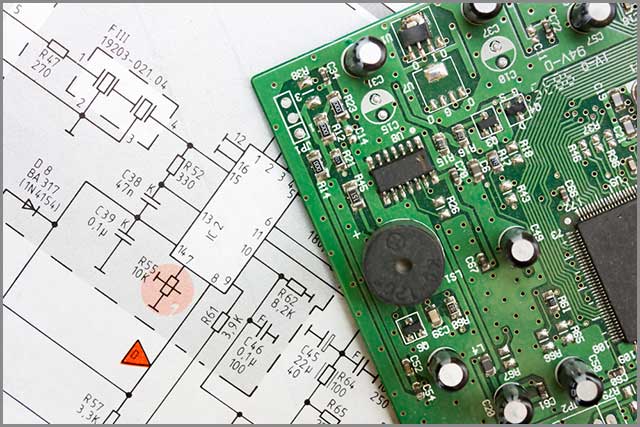
Check PCB Editor for Required Features
PCB layout is the first stage of designing your circuit board. You will need to do everything using your software. That’s why it’s necessary to check for the required features. Based on your project, you may need features like-
1. Route – to convert air wire into trace
2. Via – create vias to carry signal
3. SMD – surface mounted devices for PCB
4. Break – include corners to a line
5. Polygon – add polygons using text commands
The features will vary depending on the tool you use. However, all PCB design software will have features to create a PCB. So, check if you have got all the features.
Choose Your Ideal Board Size
When you convert schematic to PCB layout, you will have a free-sized board. The components of your schematic will be on one side. On the other hand, there will be an empty board.
Now, you have to design and place your PCB components on the board. After you have done that, check if there is any free or unnecessary space on the PCB layout. Especially, check around the borders.
If you find free space, then shrink the size of the board in your software. Having the right size PCB saves both cost and space.
Did You Place All the Components?
Not all PCBs have the same components. Your components will vary according to the application. Nonetheless, it would help if you didn’t miss out on the required components.
Create your PCB layout and include the components carefully. You may need to include pads, vias, through-holes, and SMDs. Take your time and add each component with concentration.
Before you finalize your layout, could you give it a check? See if you have included all the components. Check if anything is there on the schematic side. Also, check if the components are at their designated places.
This step is crucial to ensure the success of your project.
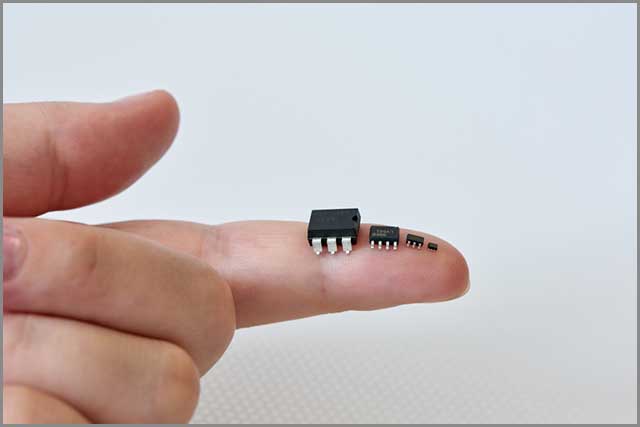
Check Your Signals to Determine Routing
Your signal paths decide the quality of your PCB. Mess up the signals, and you have an improper routing.
Signals can take different paths. You may design a PCB with straight paths. Or, you may also use a curved design. Your application and components decide the signal path you need. Many times, you may need to use a combination of straight and curved designs.
Sometimes, the PCB components also impact the choice of signal paths. Many engineers prefer straight paths for GND. On the other hand, transistors may be okay with a curved path.
Check your PCB and your connection paths. Choose the best signal path for the best results.
Determine the PCB Design Rules
It is another important consideration for converting schematic to PCB layout. It would help if you chose the right design rule for your PCB design.
Design rules also vary according to your project. For example, a design rule for PCB hobbyists can use large spaces and big traces. However, a hobbyist design rule is not appropriate for commercial PCBs. You will want to reduce space-use to save on production costs.
So, choose the right design rules for your needs.
All PCB design software will have options to change the values manually.
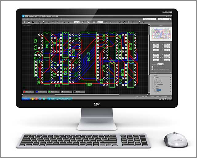
Do You Need Power Planes?
Power planes denote big areas of copper that deals with a signal. Generally, power planes carry power and ground connections. Before you convert schematic to PCB layout, decide if you need power planes.
If you are making multi-layered PCBs, then there are more considerations. You can dedicate a whole layer to making power planes.
In PCB design tools, you will be able to use commands to create power planes. Some solutions may also offer visual methods. You will need to create the power planes while the tool connects them to the signal.
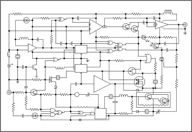
Clean Up Your PCB Layout
Before you finalize your PCB design, check it thoroughly. You might come across errors and mistakes.
Also, clean up your PCB. Look for things that you can improve. For instance, make the traces neater so that you can enjoy better clearance. Additionally, see if everything fits properly inside the layout.
Check your connections and all components. See if they are in the right places. Spend enough time to give your PCB layout a thorough examination. It will reduce production errors and improve the efficiency of PCBs.
When you finish cleaning up your PCB layout, proceed to assess your PCB.
Do not Forget to Run DRC.
It is one of the most crucial steps of creating a PCB layout. You need to check if your design rules are up to the mark or violate rules.
In step 6, you chose a design rule set for your PCB. Now you need to run the design rule check. The test will check your PCB design and determine compliance. If you need to make any changes, do it now. Adjust the design values according to your specifications. Then run the test.
A PCB layout that passes DRC is fit for production. You can run DRC and then move on to the final stage.
Export Your PCB Layout
The last thing you should do is to export your layout. You will need to contact a reliable manufacturer who will produce the PCBs for your project. The manufacturers generally need PCB manufacturing partner about their requirements.
Be sure to save a copy of the PCB layout at your end. That will help both you and the manufacturer stay on the same page. You can also match the prototype with your design. Then you can place the order for the final batch of PCBs.
Summary
We hope you are now aware of the most crucial aspects of converting schematic to PCB layout. The first thing you need is a PCB design tool to create your layout. Next, you need to place your components and design the layout as per specifications. Then you can run a DRC to test if your design meets the rules.
All through the PCB design steps, you should be careful to avoid errors. If you want, you can also get your layout done by professionals. At Wiring, we have state of the art technology. We produce our PCB with the latest equipment. And we can customize them as you need.
Get in touch with us to convert your schematic to the PCB layout. WellPCB also manufactures high-quality PCBs matching your design for the best results.

