Abstract
PCB stands for Printed Circuit Board, a copper etched board that keeps printed the laid copper tracks. These tracks connect the components in most electronics items. The board is stiff enough so that it can mechanically support components mounted over it. The panels are designed on computer-aided design software in everyday practice, and then the design is transferred over the PCB material for etching.
The etching is a chemical process where the necessary copper is saved, which removes extra copper. The printed paths after etching are known as tracks. Over etching obliterates the traces or breaks the connections resulting in an open circuit. The unnecessary open circuit or short circuit of two conductive paths results in partial or complete board failure. On the other hand, insufficient etching results in minor hair-like copper shortages from one track to another.
This is why the precision processing machines perform the board etching under controlled pressure, time, and chemical composition. Most PCBs are manufactured by fiberglass or glass-reinforced plastic materials with a copper sheet on one side. The conductive paths, i.e., tracks, are made on the copper sheet side. The components are also soldered on the copper sheet side.
Complete PCB–Content
The PCBs in the current electronic products market range from single layer, double layer, and multilayer formats. In a multilayer PCB, multiple copper conductive layers are stacked and glued over each other to enhance the signal density and reduce the PCB size. The different layers are etched and separated by the prepreg material and then joined together. The PCB sheet is an insulating sheet of 1 to 2mm thickness coated with copper on one or both sides in the raw form.
The copper is coated over the entire insulator sheet in a small quantity, like 1 to 2 ounces per square foot. In common, the copper thickness varies from 17 to 70µm. The high current sink or source circuits like power supply circuits need thicker and wider copper tracks, whereas low power but high-frequency signals need thinner copper tracks. Therefore, the magnitude of current flow is determined from the thickness of the board and the width of the copper track.
In the electronics market, various PCBs are produced categorized by performance, availability, manufacturing facility and cost, etc. The insulator material of the PCB, although not conducting, also affects signal health. It is why, for higher frequencies, unique PCB materials are used. For higher frequencies, specially developed low absorption materials are used.
, Other readily available materials are CEM-3, CEM-4, CEM-5, FR-1, FR-5, Teflon, and the Roger material. In common, FR-4 is used for single, double, and multilayer PCBs manufacturing. After manufacturing, an essential qualification phase, the PCBs are inspected for surface level finishing, solder mask coating, top overlay printing, etc…
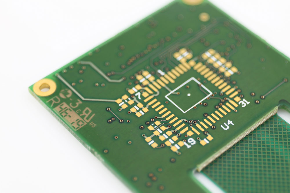
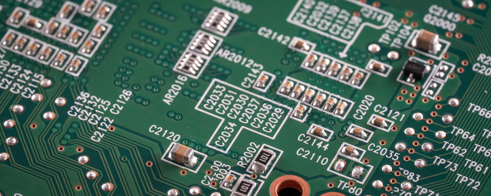
Figures 1 and 2 show different types of PCBs.
PCB manufactured for high pin density components
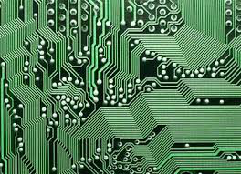
PCB tracks and vias after etching and finishing of a manufactured PCB
