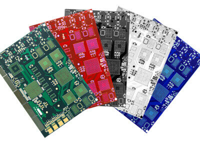
After a printed circuit board manufacturing, the copper traces on the substrate are usually at risk of oxidation and rust due to environmental exposure. The best way to prolong the board’s life is to give it a protective coating in the form of what is commonly known as a solder mask.
This article elaborates on this protection and its varieties on the market and how to use it properly to avoid issues like solder mask relief.
You also get to know how to create a mask yourself, as well as where to get custom-colored covers, finished circuit boards, and PCB assembly assistance for your project.
1. What Is Solder Mask?
A solder mask, also known as a solder resist or solder stop, is a thin layer of polymer applied onto the copper traces of a PCB to prevent oxidation when exposed to the environment and protect the copper from contaminants like contaminants, dust, and dirt.
The mask also aids in achieving good soldering results by minimizing the chances of solder bridges forming between closely spaced solder pads.
A solder bridge connects two conducting parts of a board through a small, unintended blob or whisk of solder.
You won’t always find solder masks on hand-assembled circuits, but they’re an essential component for mass-produced boards that are soldered automatically using solder-bath or reflow techniques.
In electronic design, the solder mask is treated as a separate layer of the PCB, similar to the copper and silkscreen layers.
1.1 Solder Mask Materials And Usage
Solder mask comes in different media depending upon the demands of the application. The lowest-cost solder mask is an epoxy liquid that its silkscreen through the pattern onto the PCB.
Other types are the liquid photo-imageable solder mask (LPSM or LPI) inks and dry film photo-imageable solder mask (DFSM).
LPSM can be silkscreened or sprayed on the PCB, exposed to the pattern, and developed to provide openings in the design for parts to solder on the copper pads.
DFSM is vacuum laminated on the PCB then presented and developed. All three processes typically go through a thermal cure of some type after the pattern is defined, although LPI solder masks are also available in Ultra Violet (UV) cure.
Here I will introduce solder mask materials in three media types – Epoxy liquid, Liquid Photoimageable, and Dry-film Photoimageable masks. The best option for your PCB depends on your application, as well as the amount of money you intend to spend.
1.1.1 Epoxy Liquid
Epoxy liquid, the cheapest type around, is silkscreened onto the PCB pattern. Silk-screening is a printing technique that involves the use of woven mesh to support ink-blocking habits. The mesh creates open spaces for ink transfer.
While artists often use silk, synthetic fibers with similar textures have become commonplace in electronic applications.
1.1.2 The Liquid Photo-Imageable Solder Mask (LPSM)
LPSM is delivered as an ink formulation that can be silkscreened or sprayed onto a board before being exposed and developed. Hot air surface leveling (HASL) is one particular process that is common in LPSM masking.
HASL involves using high-pressure water or vapor sprays called developers to make the mask uniform on the surface.
How is LPSM Applied?
1. The production panel is thoroughly cleaned to ensure no dust particles are trapped under the mask.
2. The panels are completely covered on both sides with the liquid mask.
3. The coated panels are placed in an oven to tack-dry the mask just enough to finish processing.
4. A film is made of your solder mask Gerber files, one for each side of the board. Where you want a cover to stick to the board, the film will be transparent. Where the mask should be removed will be black in the movie.
5. The tack-dried boards are placed into a UV developer, and the film is precisely aligned over the board. The blacked-out locations on the film prevent the UV light from curing the mask where it is not wanted.
6. After the mask is exposed to the UV lamps, the uncured cover is washed off, leaving the show only in the places needed.
1.1.3 Dry-Film Photo-Imageable Solder Mask (DPSM)
DPSM has to be vacuum-laminated on the PCB before being exposed and developed to avoid trapping air bubbles. After setting, the mask creates openings, and copper is layered inside the holes and on the traces using electrochemical processing.
Tin is sometimes also applied to protect the circuitry.
Photoimageable solder resists are generally the acceptable mask types for modern PCB designs. The surface topography of your board will dictate whether to use liquid (LPSM) or dry (DPSM) application.
Applying a dry-film mask can give you a uniform thickness across the surface, but it only adheres best if a board is exceptionally flat.
LPSM won’t result in an entirely consistent layer, but if the PCB has complex surface features, it provides better contact with the copper traces than DPSM.
Solder masks typically go through a thermal curing stage after the PCB pattern is defined, but LPSM masks can also be hardened in UV light.
1.2 Solder Mask VS. Paste Mask
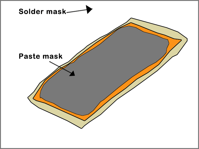
Figure 1: Solder mask and paste mask on a PCB
Solder masks and paste masks are often mentioned in the same setting, making it challenging for beginners to draw a line between them.
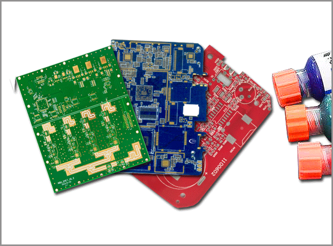
If you’ve ever seen a PCB, you’re undoubtedly familiar with its predominantly green coloring. This thin green protective coat on the top and bottom surfaces of a board is the solder mask. Despite their importance, solder masks aren’t a critical necessity for all PCBs.
There can also be circumstances where you want a mask on the top but not the bottom layer, or vice versa. Solder mask essentially covers the entire top or bottom surface, only leaving out the areas where components would make circuit board shopping; various things might get you confused. Whether you are going for a single-sided PCB, a double-sided PCB, or any other type of PCB, You can contact the board’s copper traces.
Paste mask, on the other hand, is a material that is applied to the areas that have been left uncovered by the solder mask to assist in the soldering process.
The paste is commonly used to connect surface-mount components to pads on a PCB during soldering. Still, it is can also work with through-hole pin-in-paste details by using a stencil, a syringe, or jet printing to apply the mask in or over the holes.
The solder paste’s adhesive properties enable it to stick a component in place, after which the board is heated, melting the mask and creating both an electrical as well as a mechanical bond between the part and the surface.
So, while solder mask is used, during manufacturing, to prevent the oxidation of copper traces and the formation of solder bridges, paste mask is applied, during assembly, onto the points where component pins make contact with the PCB to facilitate a firm, reliable bond between them.
Stencils made for solder mask application are different from those made for paste masks in that the former leaves uncovered the areas on a board that the latter covers, and vice versa.
The paste mask is typically gray, but as you can learn in the next chapter, a solder mask is available in many colors.
2. Solder Mask Colors
Although the solder mask has been exclusively green for a while, more shades are emerging to cater to designs with specific color requirements. To make prototype runs and revision changes more identifiable, merely make a PCB look trendy in a see-through enclosure.
With OEMs increasingly embracing clear electronics and appliances, circuit board manufacturers are adopting colored solder masks as a way to give their boards a bit of a personality.
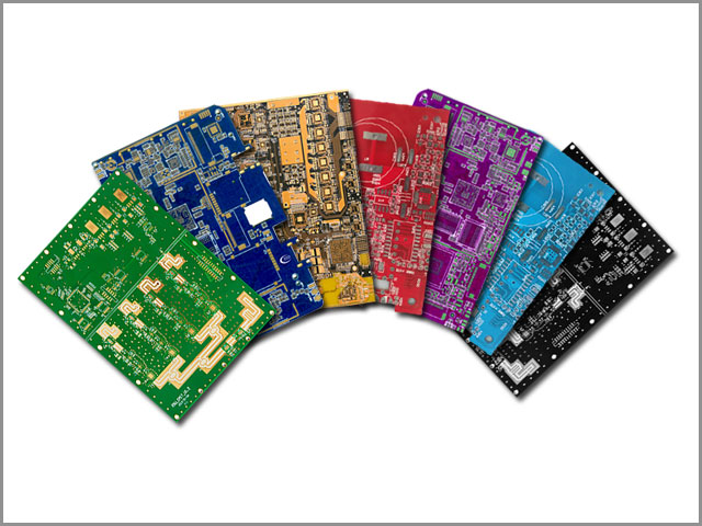
Figure 2: Solder mask colors
2.1 Commonly Used Solder Mask Colors
Today, the most widely used colors are red, blue, black, white, and yellow. Clear – not technically a color – is also a shade of choice for designers. And manufacturers can also synthesize other decisions, such as purple, orange, or even pink, from the three primary colors – red, blue, and yellow.
Green
Although the color spectrum for solder masks has expanded significantly in recent years, most PCBs still come covered in the green mask. One of the primary reasons why green is the preferred color for many designers is that it aids in the inspection.
According to research, the eyes are more sensitive to green than colors like yellow, white, or black, making it easier to see the contrast between copper pads, traces, and empty spaces.
Additionally, the green mask adheres relatively evenly, cures appropriately, and has a higher resolution than most colors. This means it can create smaller mask dams for a more space-efficient circuit.
Figure 3: PCBs with green solder mask
Red
Designers, especially those in modern niches like Artificial Intelligence and the Internet of Things, increasingly embrace red solder masks for aesthetic purposes. In some circuits, red can also give a more striking color contrast between a board’s components and traces and silkscreen.
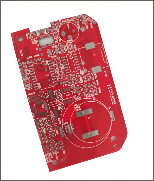
Figure 4: PCB with red solder mask
Blue
Blue and green solder masks are very similar in functionality, but for some PCB users, blue takes the win because of its uniqueness. Boards covered in the blue front are pretty rare on the market. But if you want them for your project, you can get them from a manufacturer like WellPCB.
Figure 5: PCB with blue solder mask
Black
While not exactly the most eye-catching, Black solder mask can be advantageous in applications that require light reflection. Also absorbs heat more readily than other colors, and that means it needs less heat during reflow.
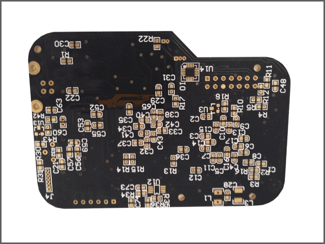
Figure 6: PCB with black solder mask
White
White is the most unpopular PCB solder mask color because it provides the most negligible visibility. Moreover, some low-quality masks start to turn yellow after a while, especially when consistently exposed to heat.
Nevertheless, white masks are often the first choice for LED systems because they’re brighter than other PCB colors.
Figure 7: PCB with white solder mask
Other Colors
If none of the shades above float your board, you can consider rarer but more uniquely appealing solder mask colors like yellow, orange, and purple. These colors are popular among companies that make niche electronics and designers looking to make their new products stand out in the market.
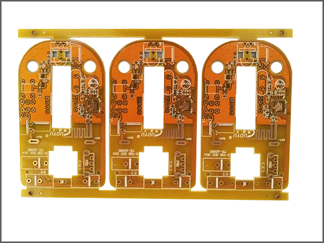
Figure 8: PCB with yellow solder mask
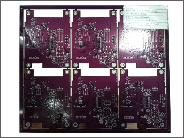
Figure 9: PCB with purple solder mask
If you want an exceedingly compact circuit, a transparent mask will give you the most miniature mask dams and mask reliefs compared to other colors.
2.2 Choosing The Right Color
Although experimenting with different shades can make your project look a lot more interesting than with the standard green, it pays to know that the color you choose will, to some extent, impact the performance of your solder mask.
For starters, black, white, and yellow are known for their poor resolution because UV light doesn’t always penetrate the entire coating. A PCB masked with these colors will have fewer tracks than a similarly-sized board with a green, red or blue mask.
On the flip side, although transparent solder masks give the highest resolution, they’re susceptible to color shifts during the many thermal excursions and chemical treatments a PCB encounters.
The performance of a color type is also determined by the quality of the solder mask itself. Top suppliers usually have custom shades that provide high resolution, as well as temperature and chemical resistance.
Designers often use different-colored solder masks for mere aesthetics. Still, if you don’t have specific color considerations, various shades can help you identify your boards during assembly and beyond.
You can use red, blue, and black to mark different prototype stages of the design and then settle on green or white for the final product.
Design Tips
The solder mask may not be a crucial requirement in PCB manufacturing but not using it can result in many problems that will significantly reduce the board’s lifespan. Therefore, if you’re designing, it is critical that you seriously think about the solder mask you would like your manufacturer to apply.
3.1 Type And Thickness
Choosing the appropriate mask will depend on several factors, most significantly the dimensions of your board, the surface layout, components, conductors, and the final application of your product.
Suppose you’re working on a project for use in regulated sectors like medicine, telecommunication, or aerospace. In that case, your solder mask of choice will also be determined by industry standards and other specifics.
Liquid photo-imageable solder masks are by far the most common types of masks today. They’re reasonably priced, reliable, and as mentioned earlier, they better know more about the defects and probable solutions to PCB problems? Contact with the PCB surface than dry-film masks.
The thickness of the solder masks primarily depends on the width of the copper traces on a PCB.
Generally, you’ll want about 0.5 mils of mask over the copper. A liquid cover typically gives varying thicknesses over the board. It can be as thick as 1.2 mils over empty laminate areas and as thin as 0.3 mils over complex features, such as the knee of a circuit.
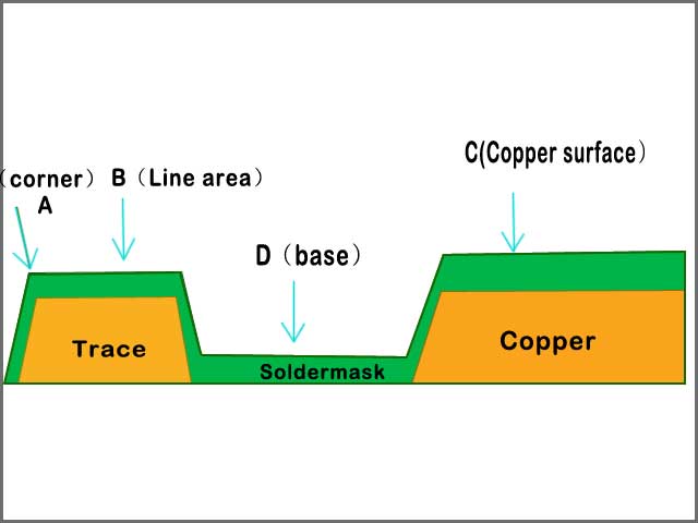
Figure 10: Solder mask thickness
3.2 Including A Solder Mask In Your Design
PCB design requires that the solder mask be its layer in the Gerber (CAD) files. The mask layers in Gerber data are negative images, which means that the front won’t cover the colored areas. In other words, the mask file will show you the places where you don’t want the mask applied.
A good rule of thumb to follow is to cover the entire board with solder masks and only leave out the areas your components will go, and perhaps the spaces you may want to use as test points.
Mask apertures will depend on your product, but ideally, the solder mask is adjusted to be 4 miles wider than the copper pad (2 mils wider per side).
If the mask is printed precisely the same size as the pad, it would likely not be centered correctly, and that can result in some of the copper pads is going to cover with the mask.
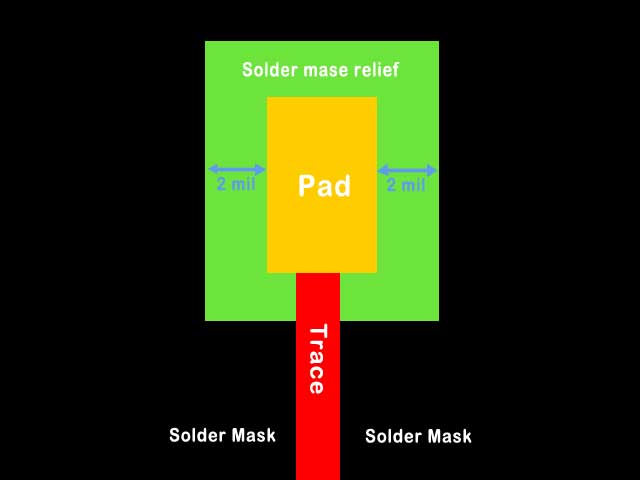
Figure 11: Solder mask relief standard
On some occasions, a project can require a mask-defined pad formed when the solder masks relief – the area on a PCB surface left without solder mask to allow components to know more about the defects and probable solutions to PCB problems? Contact with the copper pad is the same or smaller size than the pad it is exposing.
Narrow mask apertures are typically used when mask dams are required between pads, but there isn’t enough space to have a barrier and still follow the 2-mil-border standard.
Your PCB manufacturer will need you to include a fab note in your Gerber file if you require a mask dam, but you don’t want to modify certain apertures.
3.3 Avoiding Solder Mask Relief Issues
Solder mask relief areas usually surround surface-mount pads, through-hole pads, test points, and vias as margins of error during fabrication. In contrast, the mask space between two adjacent reliefs is called the solder mask dam.
The manufacturable solder mask dam measurement depends on the mask’s resolution, which is itself dependent on the color.
Shades with a low resolution like black, white, and yellow will be unable to adhere to the surface in tiny area sizes, and that means the board will have fewer pads than if it had a higher-resolution mask color.
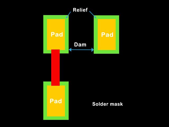
Figure 12: Solder mask relief and dam on a PCB
For a given size of a PCB, the larger the solder mask relief, the smaller the solder mask dam between the pads. In some designs, large reliefs can shrink the barriers beyond the allowable size, exposing more copper than is allowable and creating the risk of solder bridging during assembly.
On the other hand, too little relief can result in the contamination of pads by the solder mask, making the surface uneven and difficult to solder.
Solder mask relief problems can avoid by keeping the reliefs on your design to the standard 2-mil border. It also pays to keep in mind the color of the mask you’re using. High-resolution shades like green, red, blue, and transparent can accommodate smaller dams and smaller reliefs (ideally 1.5 mils per side) for a more compact pattern.
4. Manufacturing PCBs With Custom Colored
Applying a solder mask onto a circuit board is a tricky and demanding endeavor. Boards are known to fail due to solder mask issues like insufficient or extra-large mask reliefs or few or excess holes. Nevertheless, as the following DIY guide will show you, masking a PCB on your own is not impossible.
4.1 How To Solder Mask A PCB At Home
If you often make prototypes with old unmasked boards, knowing how to apply a solder mask can be a beneficial addition to your skillset. You can also save a significant amount of money by buying “naked” PCBs and doing the job yourself, depending on your board supplier and the size of your project.
Below is a list of the supplies you will need to mask a PCB.
- UV Curable Solder Mask Resin
- Transparent Film
- Nitrile gloves
- Isopropyl Alcohol
- X-Acto knife
- Ruler or T-square
- Cutting Mat
The essential items are the UV curable resin and the transparent film. UV curable resin hardens when exposed to ultra-violet light and is, therefore, a more sensible choice than thermal-cured mask materials.
The resin comes in different colors, and you can purchase it online or from a local electronics hobby store.
Making A Template
The first thing to do is to create a solder mask template using the transparent film. If your PCB design is simple, you can manually cut out the template by overlaying the film over the board and marking the pads and vias with a fine-tipped sharpie.
For more complex designs, use your CAD software to print your PCB layout onto the film. Designers commonly use inkjet printers with special “Quick-Dry” type transparency paper to draw out a template.
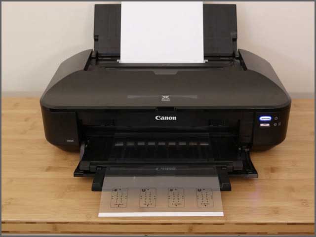
Figure 13: Printing a mask template with an inkjet printer(picture from adafruit)
Prepping The Film
Using your X-Acto knife, cut out the template from the paper, leaving some space around the edges for easy handling. You will need to add another printed template on top of your first one if the link doesn’t seem dark enough to block UV light.
Perfect alignment between the two sheets is crucial, so glue the edges together to stay in place.
Prepping The PCB
Before applying the resin, make sure your PCB is clean and rust-free. You can use a Scotch Brite pad to brush the board lightly and remove oxidation.
Applying The Resin
Place the clean board down on a new transparent film and use your fingers to press out the resin from the tube and onto the PCB surface. Use your best judgment to apply the amount of wax that will cover your entire board when you spread it.
Place another film on the PCB and squeeze down lightly to spread the resin. You can use your finger or a squeegee to make sure the wax reaches every corner and eliminate any air bubbles that may form.
Placing Your Template
When you’re satisfied with the resin application, set the film containing your template over the PCB and take your time to line it up correctly. You can add a drop of alcohol to the back of the template to adhere better to the film on the PCB.
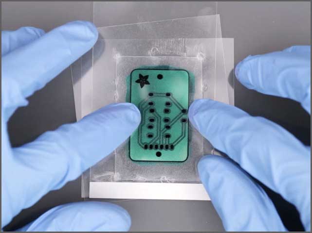
Figure 14: Perfect template alignment is key(picture from adafruit)
Exposing The Resin
Shine a consistently bright UV light source like an LED flashlight or lamp on the PCB. The light source you use should be large enough to cover the entire surface at once so that all board areas are exposed uniformly.
Peeling The Film
After exposure, carefully peel off the layers of film from the PCB. If you had exposed the resin enough, it would have hardened onto the board, and only the sections blocked by the ink on your template will be wet. You can then wash off the sticky resin to fully uncover the unmasked parts.
4.2 Factors To Consider When Masking A Board
As you have probably realized, masking a board demands a considerable deal of professionalism. To create a solder mask template for your PCB, you will need to take the utmost care to find the perfect alignment since a mistake can cause the mask to cover unintended areas.
You must also watch the sharpie or printer ink you use so that it’s dark enough to reflect UV light effectively, not to mention your type of light source, and how long to expose the resin so that it hardens sufficiently on the board.
Because of these overwhelming factors and the time required, most designers contact PCB manufacturers for their masking needs. Seeking professional help will be a better option for you than a DIY masking job, especially if you want a product that will stay functional for the long run.
If your project is sensitive and you wish to avoid costly mistakes, consider sending your files to a manufacturer and having the PCB made for you with the solder mask you want, rather than attempting to mask it yourself.
WellPCB Can Help
WellPCB is your one-stop shop for everything PCBs. You can be ready to use your Gerber files to deliver the boards you want for your project. Regardless of your preferred solder mask color or the specifications, you include them in your fab notes.
The company will meet your demands with unrivaled accuracy. Thanks to its rich manufacturing experience, mature technologies, and up-to-date equipment.
So, don’t let improper solder mask application be what undermines your project. Contact WellPCB and let them handle everything for you.
