Many JFET types exist today. Each of them provides special features/specifications, which present various circuit applications. Now, in this article, we will discuss the 2N3819 JFET. This device can handle medium to high range frequencies while providing high gain for wideband frequencies. It also offers signal amplification, fast switching, and mixing capabilities for many different applications. Furthermore, this device integrates audio systems, providing enhanced sound.
Understanding this small N-channel junction Field Effect Transistor and how it works can seem confusing. That’s why we wrote this simple article, which aims to put you on the right path. So let’s get started!
Contents
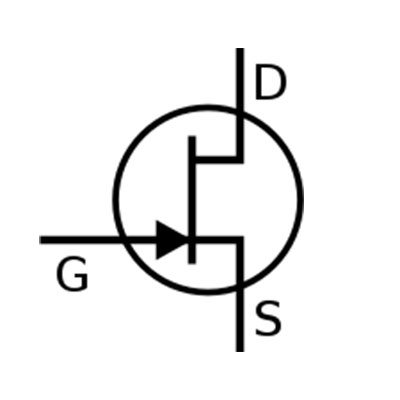
Pin Description of 2N3819 JFET
We described the 2N3819 pinout in the table below:
| Pin Number | Pin Name | Description |
| 1 | Source | JFET source pin |
| 2 | Gate | JFET gate pin |
| 3 | Drain | JFET drain pin |
Features and Specifications
| Parameter | Symbol | Value | Unit |
| Drain-source voltage | VDS | 25 | Vdc |
| Drain-Gate voltage | VDG | 25 | Vdc |
| Gate-Source voltage | VGS | 25 | Vdc |
| Power Dissipation | PD | 350 | mW |
| Drain Current | ID | 100 | mAdc |
| Max Forward Gate Current | IG(f) | 10 | mAdc |
| Storage and operating temperature range | Tstg | -65 to +150 | °C |
You should note that this device supports a 100mAdc drain current, an important feature. Hence, it should be utilized in applications as a switch when the drain current reaches less than 100mA.
2n 3819 Working Principle
The 2N3819 contains a conduction path from the source and drain. Restricting charge flow from the source to drain terminals occurs by calibrating the channel path’s area.
A field-effect produces the conduction channel. Applying a positive voltage to the gate and source terminals will cause the pn-junction to operate in reverse bias. As a result, the depletion region, which forms around the gate terminal, expands. Then, the depletion region produces a gradient surrounding the pn-junction. Therefore, this restricts current flow to the source and drain, achieved through narrowing the conductive channel’s width.
Conductivity from the source to drain ceases when the depletion layer surpasses the conduction channels width. The pinch-off region refers to stopping the conductivity. For example, applying a negative voltage to the gate-source will cause the N-Channel JFET to stop functioning. However, damage can occur if stresses overtake the absolute value. Additionally, applying stress for too long can affect its reliability.
2n 3819 Alternative Options
We listed 2N3819 alternatives below:
- 2N4416
- NTE312
- 2N5638
- 2N5640
- 2SK162
- 2SK518

Applications of 2n 3819
A 2N3819 JFET integrates on an RF circuit
Below are applications for the 2N3819 JFET.
- Signal modulation
- Audio amplifier systems
- Low noise
- Low signal amplification
- Radio Frequency module
- High-speed analog switching
- Sensor circuit
- VHF/UHF mixers
- Receiver and transmitter
How to Choose a JFET
Ensure that you follow these guidelines when choosing a JFET:
1. You should ensure that the JFET suits the application. The N-Channel JFET, utilized on the power path, represents 2N3819. However, we recommend a P-Channel for high-side switching applications.
2. Perform drain current calculations. In fact, a JFET capable of handling more than the application’s drain current will suffice. The 2N3819 operates with a maximum drain current of 100mA.
3. You will need to select a JFET that handles more than the required drain-source and gate-source breakdown voltage. The 2N3819 is compatible with 25V gate-source breakdown voltage and 25V drain-source breakdown voltage.
2n 3819 Circuits Examples
N-Channel JFET as a Switch
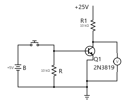
Circuit diagram showing the N-channel JFET as a switch
The DC voltmeter, connected between the drain and source terminal, measures voltage. After the gate terminal’s N-channel receives zero voltage, the FET switches to saturation mode. Consequently, this results in a closed circuit. Therefore, the DC voltmeter will read that nearly zero voltage emerges on the drain terminal.
Applying sufficient negative voltage to the gate terminal causes the FET to function in the cut-off region. As a result, it works as an open circuit. Meanwhile, the DC voltmeter will display the input voltage source (+25V) for the drain terminal.
Audio Mixer 2N3819
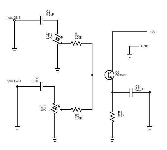
Circuit diagram of audio mixer with the JFET 2N3819
Both audio input channels attach to the transistor gate along with two capacitors and variable resistors. Applying input signals to the mixer causes the gate voltage and drain current to vary. Then, it alters the load resistor’s voltage drop, amplifying the audio signal.
Each variable resistor contributes to audio mixing. Changing the resistances allows controllability over the input channels via both boosted signal and mixer output. In effect, this process produces different sound levels. Finally, connecting a capacitor in the output provides a high-quality signal.
Summary
Overall, the 2N3819 JFET device provides low-level signal amplification and switching capabilities. This means that it will help improve the signal on an electronic circuit, especially for VHF/UHF mixer applications. Additionally, you can see that the 2N3819 supports 25V Drain-Source and Gate-Source breakdown voltage. This means that it’s sufficient for applications that handle more than the required breakdown voltage. The device operates by restricting current flow to the source and drains pins, which occurs while narrowing the conductive channel’s width.
Do you have any questions regarding the 2N3819 JFET? Feel free to contact us!