A 565 phase-locked loop is a regulatory system that produces an output signal phase related to the input signal phase. Some types might include a phase detector in feedback loops and a variable frequency oscillator.
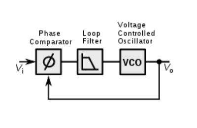
Simple analog phase-locked loop
Source; Wikipedia
LM565 IC is a general-purpose phase-locked loop chip consisting of a phase detector and a voltage-controlled oscillator. As we expound on the article, you’ll get to appreciate LM565 IC features, block diagrams, applications, among others.
Contents
lm565 pinout Configuration
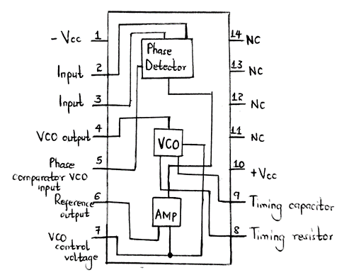
LM565 PLL has fourteen pins whose functions we’ll discuss below.
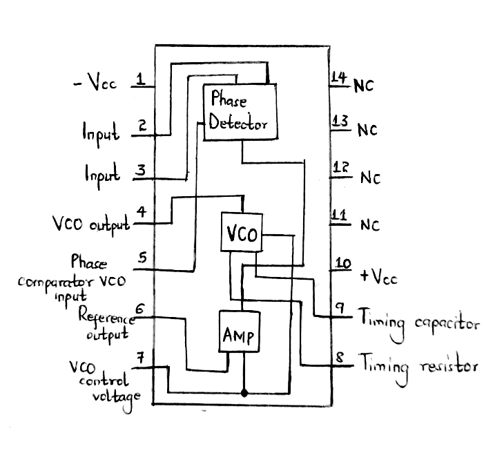
The LM565 pinout
Pin1/ -Vcc – The input pin has a negative power supply.
Pin2 and pin3/ Input are the FM signal or phase detector input pins.
Pin4/ VCO output – The pin functions as the Voltage control oscillator (VCO) output.
Pin5/ Phase comparator VCO input – The phase detector input pin feedbacks VCO output.
Pin6/ Reference output – The pin signifies an internal amplifier reference output.
Pin7/ VCO control voltage – You can get the VCO control voltage through this pin.
Pin8/ Timing resistor – The resistor pin free-runs VCO frequency.
Pin9/ Timing capacitor – The capacitor pin is for free running the frequency of VCO.
Pin10/ +Vcc – It is the positive power supply pin.
Pin11 to pin14 – The four pins have no connection.
LM565 features /specifications
We will now take through the specifications and features of the LM565 IC.
- First, it has a wide power supply range and a power supply current of 12.5mA.
- Then, its operating voltage range is from ±5V to ±12V (maximum supply voltage).
- Thirdly, its maximum power dissipation is 1400mW, and it has a VCO maximum operating frequency of 500KHz.
- Also, the VCO has a frequency stability of 200 ppm/°C.
- The PLL has a 0.2% linearity of demodulated output.
- Its storage temperature ranges from -65°C to +150°C, whereas its operating temperature ranges from -55°C to +125°C.
- Lastly, it is available in a linear triangle wave having phase zero crossings. It is also compatible with DTL and TTL square wave output and phase detector input.
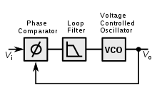
Block Diagram of PLL & Working Principle
- Phase-Locked Loop (PLL) components
A phase-locked loop (PLL) often comprises the three blocks listed below;
- An active low pass filter,
- A phase detector, and
- A voltage-controlled oscillator (VCO).
Block diagram of PLL

Simplified block diagram of LM565 PLL
The diagram shows that you can apply the phase detector output as an active low pass filter input. At the same time, using the active low pass filter output as VCO is applicable.
Working as a PLL
Briefly, PLL works in the following ways;
- It starts with the phase detector (PD) generating a DC voltage proportional to a difference in phases. The difference is between a feedback signal or output (fout) and the input signal frequency of fin.
- Since PD functions as a multiplier, you will get two frequency outputs as frequency differences in fin and fout and (fin+fout).
- Later, an active low pass filter amplifies the signal. Additionally, it generates an output DC voltage after removing any high-frequency component from the phase detector output.
- Lastly, if you apply no input, the VCO provides a signal with a specific frequency. You can also provide a DC voltage to the frequency to shift it on either side. Thus, the DC voltage at the low pass filter output is directly proportional to the frequency deviation.
Note; The process will run until the input signal frequency equals the VCO frequency.
PLL modes of operation
The three modes by which PLL operates include;
- Capture mode,
- Lock mode, and
- Free-running mode.
In the beginning, when there’s no input applied to the PLL, it works in a free-running mode. After applying some frequency, the output signal frequency of VCO in the PLL changes into the capture mode. Finally, if the input signal frequency equals the output signal frequency of VCO, PLL operates in the lock mode.
IC 565 Pll Block Diagram
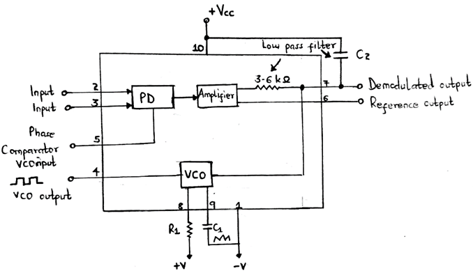
Block diagram of LM565 PLL
565 Phase-Locked Loop: Block diagram explanation
The block diagram of IC 565 includes a VCO in a feedback loop, an amplifier, a low pass filter, and a phase detector.
The phase-locked feedback loop has no internal connection. Hence, you’ll need to externally connect pin4 (VCO output) to pin5 (phase comparator input).
When applying IC565 in frequency multiplication applications, you’ll insert the digital frequency divider between pin5 and pin4 (in the loop).

lm565 Similar ICS
Alternatives or replacements of LM565 IC can be 74LV4046A, 74HCT9046A, MAX2880, and MC1648.
565 Phase-Locked Loop: How to use LM565 IC?
To comprehend its usage, let us study LM565 IC internal block diagram.
Internal block diagram of LM565 PLL chip
565 Phase-Locked Loop: Explanation
- First, pin3 and pin2 are the input pins that help us connect the input analog signal. However, since pin3 remains grounded most of the time, pin2 acts as the input.
- The input signal and VCO feedback/VCO output proceed to a phase detector (PD). The PD establishes a positive output voltage in the presence of a frequency or phase. But the PD produces zero-voltage output when signals are in frequency or phase.
- Then, an amplifier receives the output voltage and amplifies the voltage signals before giving it to VCO. The VCO decrease and increases in the waveform, thereby forming a signal frequency equivalent to the input voltage’s magnitude.
- Finally, the adjustment allows the VCO frequency and input signal frequency to match.
- The VCO is in a free-running mode in the absence of input. Under the circumstances, it generates a signal with a frequency determined by the resistor at pin8 and capacitor at pin9.
565 Phase-Locked Loop: Applications
Applications of LM565 IC comprise;
- Tone decoding,
- Signal regeneration,
- FM and FSK demodulation,
- Coherent demodulators,
- Date and tape synchronization,
- Telemetry receivers,
- Modems,
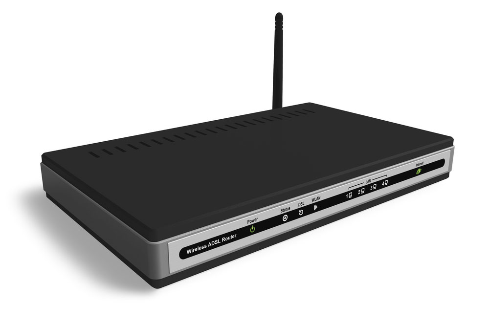
(modem router)
- SCA demodulators,
- Frequency division and multiplication, and
- Frequency synthesizer.
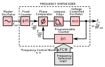
Block diagram of a type of PLL frequency synthesizer
Source; Wikipedia
565 pll Related Issues
In this segment, we will be answering some questions related to 565 PLL.
- What is the formula for the free-running frequency FO of 565 PLL?
The formula is below;
FO=1.24R1C1Hz
Whereby;
FO = Center frequency
R1 = External resistor at pin8 (value restricted between 2kΩ to 20kΩ)
C1 = External capacitor at pin9 (can be of any value)
- What pull-in time?
Pull-time is the total time a PLL takes to create a lock.
- What is VCO?
Also called a voltage-controlled oscillator refers to an oscillator circuit that applies an external voltage to control the frequency of oscillations.
- Define capture range and lock range? Which is greater?
A lock range signifies frequencies’ ranges that enables the PLL to maintain lock (and track changes) with the incoming signal. Conversely, a capture range is the range of frequencies whereby a PLL can obtain a lock with input signals.
Of the two, a lock-in range is greater.
Conclusion
We’ve come to the end of our blog, and we hope you are more knowledgeable about LM565 PLL. For more questions, kindly reach out to us. We’re always at your service.