Contents
74LS74 Pinout Configuration
The table summarizes the pin configuration of 74LS74 IC.
| Pin No. | Pin Symbol | Pin Name | Pin Function/Description |
| 14 | Vcc/Vdd | Supply voltage | It provides power of approximately 5V to the IC. |
| 7 | Vss | GND/ground | It has a connection to the system’s ground/GND. |
| 10, 4 | 2 PRE (bar)1 PRE (bar) | PRE input/ Set pin | It has a connection to the system’s ground/GND. |
| 12, 2 | 2D/1D | Data input pin | It’s an input pin for the IC. |
| 13, 1 | 2 CLR (bar)1 CLR (bar) | Clear data | It’s also an input pin of the IC flip-flop. |
| 11, 3 | 2 CLK1CLK | Clock input pin | You must provide a clock pulse for the flip-flops when using the pins. |
| 8, 6 | 1Q’ (bar)2Q’ (bar) | Complementary output pin | It’s the inverted output pin of the flip-flop. |
| 9, 5 | 2Q/1Q | Output pin | It’s the inverted output pin of the flip flop. |
74LS74 Trigger Table
| INPUTS | OUTPUTS | ||||
| PRE (bar) | CLR (bar) | CLK | D | Q | Q (bar) |
| L | H | X | X | H | L |
| H | L | X | X | L | H |
| L | L | X | X | H | H |
| H | H | H | H | L | |
| H | H | L | L | H | |
| H | H | L | X | Q0 | Q0 (bar) |
X is a representation of ‘Don’t care.’
The up-arrow is an indication of the signal’s rising edge.
The flip-flop table consists of individual set inputs and precise inputs. In addition, it also has complementary Q (bar) and Q outputs.
74LS74 Flip-flop Features

An implementation of dual-edge-triggered D flip-flop
Source; Wikipedia
74LS74 IC features and specifications are;
- First, It has an operating voltage ranging from 2V to 15V.
- Secondly, its operating temperature range is from 0°C to 70°C.
- Then, It has a bipolar input type while the output type is push-pull.
- It also has a high-level output current of 8mA and a propagation delay of 40nS.
- Its maximum low-level input voltage is 0.8V, whereas its minimum high-level input voltage is 2V.
- Lastly, you can find it in 14-pin SOT42 or SO-14 packages.
74LS74 Flip-flop Equivalents
You can also opt for the equivalents of 74LS74 IC, like the examples listed here.
- 74LVC2G80,
- HEF40312B.

74LS74 Dual-D Flip-flop Introduction
74LS74 IC falls under double D-type edge-triggered flip flops with complementary output and clear preset terminals. D stands for delay or data.
In other words, the flip flop module operates on features that help get D input value. Often, the value is at a point in the clock cycle or signal, e.g., in the clock signal’s falling edge. Eventually, you’ll get the D input data at the positive end of the pulse via the flip flop.
It stores data as binary numbers, and one of its features allows for a change in stored data when needed. Its specifications include making direct interfaces with NMOS, TTL, and CMOS and a high value of operating voltage range.
Finally, the low level at the input terminal of the preset resets the output value as per the inputs’ logic level.
How Do We Use 74LS74?
Operating a 74LS74 flip flop is simple since it’s straightforward, as we’ll show you in the steps below.
- Start by powering the IC using GND and Vcc pins.
- Then, because each flip-flop works autonomously, use the first flip-flop to connect input signals 3 and 2. Consequently, you’ll receive an output at pin6 and pin5.
Note;
Always provide pin3 with a clock source like a PWM signal from 555 timers or a Microcontroller Unit (MCU). Moreover, you can also use the pin to reset the flip flop by raising it and clearing its data.

555 timer IC
Source; Wikipedia
The function table below shows the complete operation of the flip-flop.
| INPUTS | OUTPUTS | ||||
| PRE (bar) | CLR (bar) | CLK | D | Q | Q (bar) |
| L | H | X | X | H | L |
| H | L | X | X | L | H |
| L | L | X | X | H | H |
| H | H | H | H | L | |
| H | H | L | L | H | |
| H | H | L | X | Q0 | Q0 (bar) |
Simulation
The simulation will help determine if the flip-flop IC works. In the beginning, you can use logic bits and logic status to examine the IC’s standard operation. However, you can also use actual circuitry instead to confirm the requirements.
You can incorporate the gif illustration below and combine its usage with the function table for a better outcome.
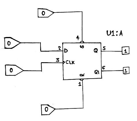
GIF illustration of practical use of 74LS74 IC
Application
You can find 74LS74 flip-flop applications in the following components/devices;

Current buffer circuit
Source; Wikipedia
- Latching devices,
- Network equipment,
- Shift registers,
- Digital electronics,
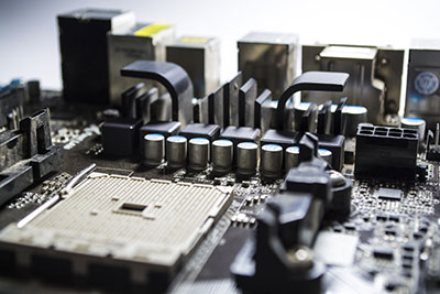
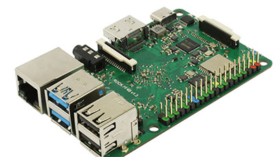
- PCs, TVs, and notebooks,
(close-up view of a typical desktop computer baseboard).
- Sampling circuits, and
- Control or memory registers.
Conclusion
In summary, 74LS74 is a high-speed D-type flip-flop with positive edge triggering. It belongs to the 74XXYY IC series and can work with microcontrollers and TTL devices (using Schottky TTL circuitry).
For further queries, kindly reach out to us.

