In electronics, there are many devices that you can use for data storage. However, none does it better than the high-speed CD4027 Dual JK Flip-Flop that we are discussing today.
We’ll cover why this flip flop is best suited for data storing in high voltages scenarios. Also, we’ll elaborate on other vital insights of the device, such as the input and applications.
Check out our guide.
Contents
What is a CD4027?

Data Boxes Illustrating the Use of the IC in Storing Data
It’s a Dual JK Flip-Flop capable of functioning at high speed and high voltage. The primary use of the CD4027 JK Flip-Flop IC is to store data. Also, you can refer to the ICs as latching devices.
It can record a single bit of data and latch the output depending on its memory. Hence, the property is helpful in applications that require small memory, like in shift registers.
CD4027 Pin Configuration

The CD4027 is a 16 pin IC like this one.
The following are the IC’s pins and their respective uses

CD4027 Features
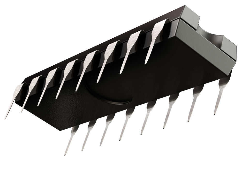
A 16 pin IC
The following are the standout features and specifications of the CD4027 IC:
- It is a Dual JK Flip Flop IC. Furthermore, the IC retails in packages of GDIP, PDSO, and 14 pin PDIP sets.
- Secondly, it has several operating voltages such as 15V, 10V, and 5V. Also, it has an operating speed of 16MHz.
- Third, it features a maximum operating voltage of 20V. But, when you supply a voltage of 5V, its input rise/ fall time will be 45us.
- Fourthly, it has maximum and minimum input voltage levels of 2V and 0.2 V, respectively.
- Lastly, it also has the set-reset capability. Additionally, it has TTL compatibility.

How to Use CD4027

Circuit Diagram
We highlighted that the J and K pins are the flip flops’ input pins. On the other hand, the Q and Q bar pins represent the flip flop’s output pins.
During connection, it’s important to pull down the input pins via a resistor of at least 1k resistance. Thus, you’ll shield the pins from being in a floating condition. Also, note that the clock signal is handy in changing the output’s state.
Thus, the flip flop changes the output only during the clock signal’s rising edge. Also, it would help if you had a truth table to decode the flip flop’s output state.
CD4027 Applications

The IC is essential in Computer Memory Circuits.
- It’s essential in the control of EEPROM circuits and latching devices.
- Also, it’s useful in shift registers and control registers.
- Lastly, they are key in memory registers.
Conclusion
We hope that we have answered all your queries concerning this IC. If you have a question, don’t hesitate to reach out to us.