Contents
CD4049 Characteristics
The CD4049 datasheet lists the performance and technical components of this IC in detail. Nonetheless, some of them are:
- A supply voltage ranges from 3 Volts to 15 Volts.
- It has a high sink current and source capabilities. For that reason, the IC can drive two TTL loads using a 5-volt supply over a complete temperature range.
- With this circuit comes a unique input protection feature. In addition, it permits a higher gate input voltage than the Vdd. Consequently, this feature prevents static discharges.
- The inverter IC has high to low logic-level conversion abilities.
- Also, the max input limit is at 1µA over an 18V complete package range of temperature. At 25°C, the max input is at 100nA over 18V.
- It has a thoroughly tested 20V quiescent current.
- Often, they come in a 16-pin package like in SOIC, PDIP, SO, and TSSOP.
- Their parametric ratings are 5, 10, and 15 volts.
CD4049 IC Pinout Arrangement and Function
In the CD4049 IC, there are 16 pins/terminals. Below, we have an outline stating the PIN and name alongside their descriptions, too.
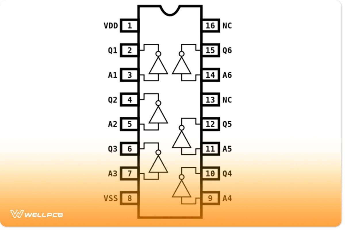
(A CMOS CD4049 diagram showing the 16 pins and their names)
- Pin 1 – This is the voltage supply terminal.
- Pins 3, 5, 7, 9, 11, and 14 (A, B, C, D, E, F) make up the inverter input pins on one side.
- Pins 2, 4, 6, 10, 12, and 15 (G, H, I, J, K, L) – On the other side, you find these inverter output pins.
- Pin 8 – This is the ground terminal of the IC.
- Pins 13 and 16 – Lastly, these are the NC (Not connected) terminals.
Applications of CD4049
Generally, there are various modes of CD4049 IC applications. Though, more specifically, we use them in converting the logic levels in a circuit. Other times, they still serve other electronic purposes, such as:
- The composition of a square-wave oscillator.
- In building DTL and TTL converters.
- For use in a voltage multiplier circuit.
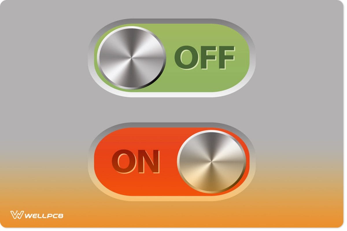
- Useful in switching or in ON/OFF circuits.
- Serves a function in current source or sink drivers.
(On and Off Switch)
Building a simple circuit using CD4049
It is sometimes a technical debate on CD4049 vs. CD4049UBE; which is a better IC? In truth, when building extreme noise fuzz circuits, you are better off with the unbuffered version.
By standard, there are constant values for the components you use in building with these hex buffers. In conjunction, both the resistor, R1, and capacitor, C1, determine the frequency, F. Thus, we portray this relationship with the formula:
F = 1 / (RxCx1.39)
Also, the ideal power source is from 3V up to 12VDC.
Further on, we are going to build a touch-on-off switching circuit with 2 CMOS Inverters. So, let us introduce two other similar circuits built using the CD4049 Hex inverter buffer IC.
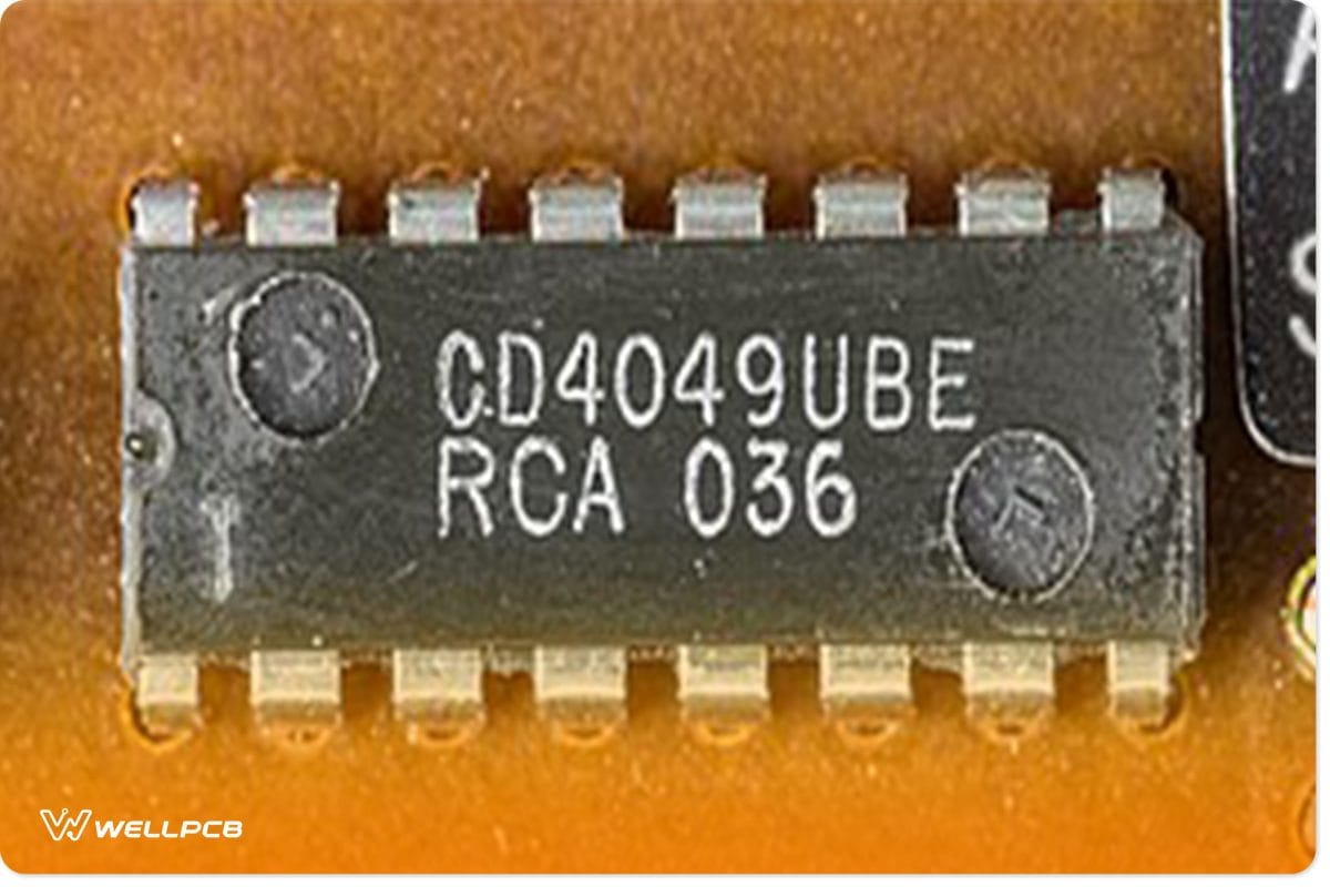
(A CD4049 unbuffered pinout installed in a circuit board)
Simple bounceless switch circuit
First of all, we look at the bounceless switch circuit. The reason it is a top pick is due to its low noise production and high quality. By default, this electronic switch circuit works in an RS flip-flop set.
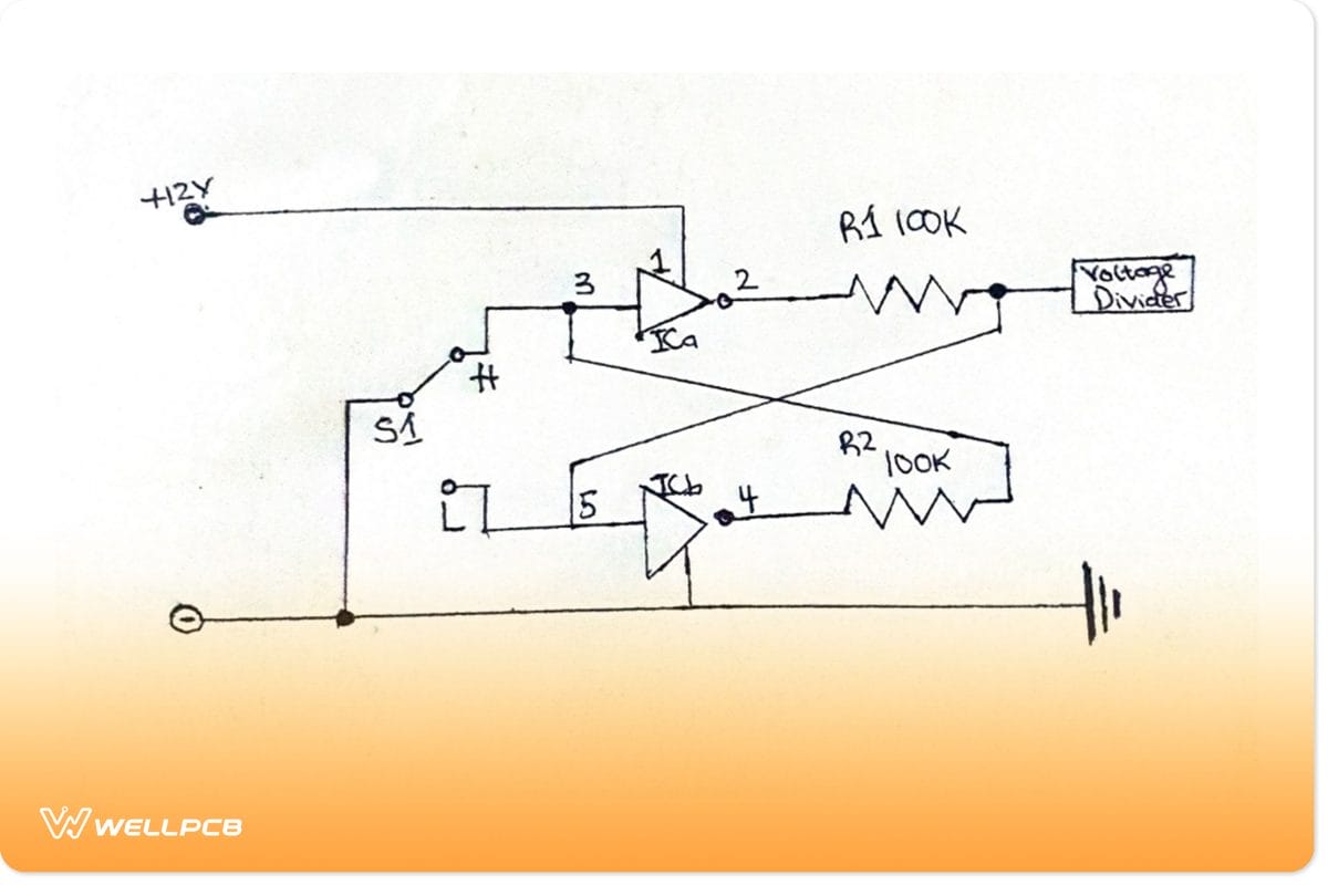
(Schematics of a simple bounceless switch circuit using CD4049)
The working principle involves constructing a circuit that locks the output signals, whether low or high. As a result, the mechanical switch releases an initial pulse. Henceforth, the circuit ignores future pulses from the control switch. As a result, the bounceless button has its output connected to the digital inverter’s input. Therefore, the control circuit receives a single pulse and not serial pulses.
Square Wave Oscillator Generator Circuit
Another example of a simple circuit built with IC-4049 is a Square Wave Oscillator Generator. Here, we introduce the CD4049 Hex Inverter for this particular purpose. Setting this up is straightforward. For starters, you only need a capacitor and a resistor. Then, your IC-4049 Hex inverting buffer makes up for what remains.
In terms of features, the square wave oscillator generator’s energy consumption is quite low. Relatively, the output frequency stays constant. On account of power supply voltage, the rates of frequency changes are also lower. Generally, these circuits have a 50% duty-cycle square wave production.
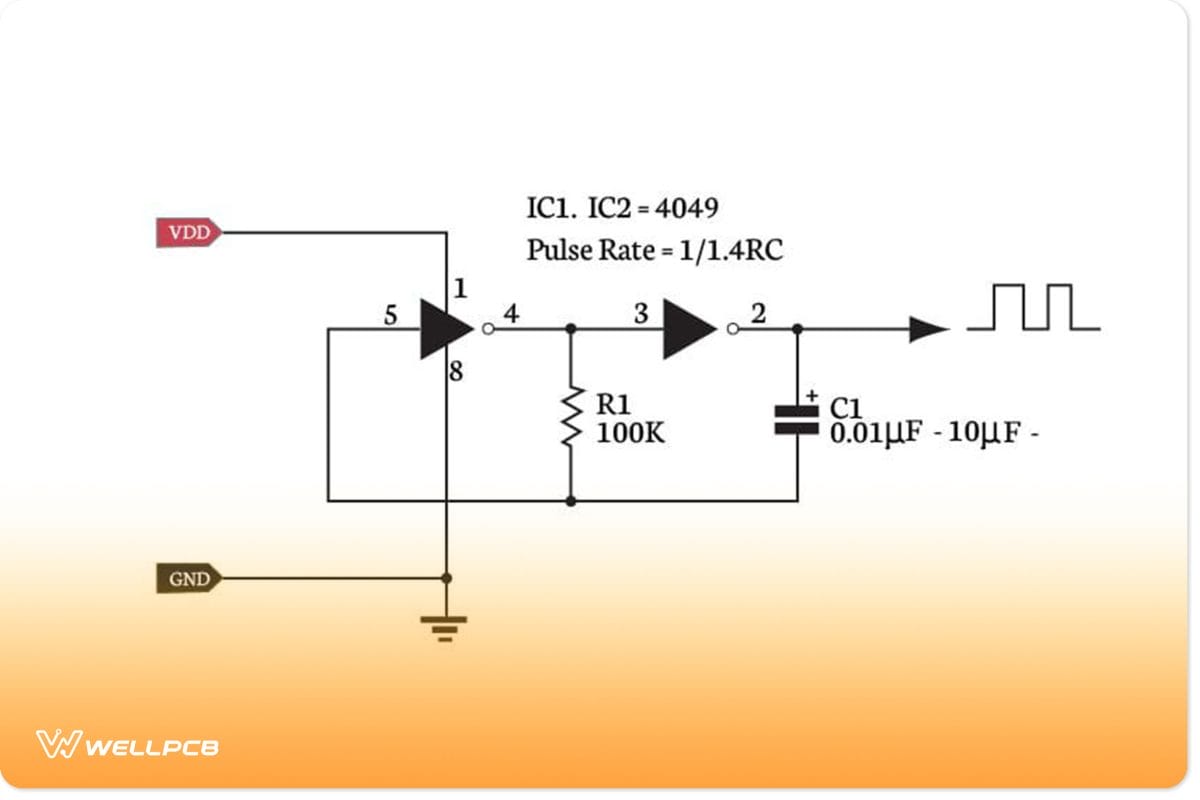
(A square wave oscillator generator circuit with CD4049)
Building a Touch ON-OFF circuit using a CD4049 Inverter IC
Herein, with this practical guide, you aim to set up an On-Off circuit to function like a flip-flop. When you touch the cable, it turns the LED On, and on another contact, the lights go off. In other words, it functions like digital sensors in the circuit. We often see this application in touch lamps.
Required Components
In practice, you need a few components to begin building your circuit.
- CD4049 Hex Inverter gate IC.
- 470Ω resistor.
- 1MΩ resistor.
- 4.7MΩ resistor.
- 100nF capacitor (ceramic).
- 1μF capacitor (electrolytic).
- LED.
- Breadboard.
- Jumper wires.
- 5V DC Power Source.

(Circuit Components with the integrated circuits visible in the background).
This IC has six inverter gates independent of each other. Note that there are pins with the mark A for clarity. These make up the inverter IC input pin, and where some pins marked with Y serve as the output terminals.
To begin, let’s prepare our Truth Table. This little chart shows the NOT logic gate IC output for any input.
| INPUT | OUTPUT |
| Low | High |
| High | Low |
In other words, for every low input (0), the output is high (1), and vice versa. It acts as the basis for how your finished circuit functions.
Connection Procedure
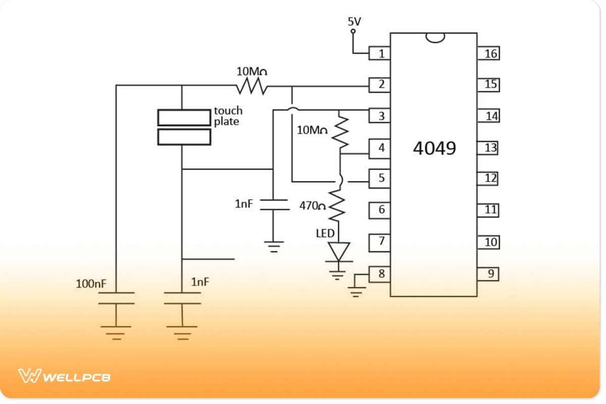
(Circuit Diagram for constructing a Touch ON-OFF circuit using a CD4049 Inverter IC)
- Getting started, you connect the power supply to the CD4049 Inverter Chip. That means connecting Pin 1 and Vdd to, let’s say, a 12V input. Then, Pin 8 and GND go to the Ground.
- Next, run the 10MΩ resistor in connection with Pins 3 and 4.
- Then, connect another resistor of 10MΩ from one touch plate’s ends to Pin 2 on the inverter chip. In a parallel connection, install the 100nF capacitor with the touch panel.
- On connecting the opposite touch plate end to Pin 3, also link the 1μF capacitor.
- Now, you connect the 1MΩ resistor between Pin 2 and Pin 3.
- At this point, you connect the first gate’s output to the input of gate 2. So, you run a connection from Pin 2 to Pin 5.
- Lastly, you install your output device. In this case, your touch On-Off device goes to Pin 4 (the second gate’s output). The LED contains a protective 470Ω resistor that prevents excessive current from burning it.
With this, you have completed your hardware connection. Finally, your circuit is ready for switching On-Off the LED.
Conclusion
Overall, the CD4049 is one model out of many other logic-level converters out there. Generally, they are digital inverters you find in various electronic applications, including dedicated digital circuits. In most cases, their functions depend on how you connect these logic ICs to other circuits.
Did you encounter any difficulties in building this circuit, or do you have questions? Reach out to us by using our contact button.