Contents
- 1 What are the Different Ways to Make a Circuit Board?
- 2 How to make a circuit board?
- 2.1 Step 1: Prepare the Tools required
- 2.2 Step 2: Get the Necessary Materials
- 2.3 Step 3: Design A Circuit Diagram
- 2.4 Step 4: Draw Your Schematics
- 2.5 Step 5: Printing Your PCB Layout
- 2.6 Step 6: Cut the Copper Plate for the Circuit Board
- 2.7 Step 7: Transfer the PCB Print onto the Copper Plate
- 2.8 Step 8: Etch the Plate
- 2.9 Step 9: Cleaning, Disposal, and the Final Touches for the Circuit Board
- 2.10 Step 10: Drilling the Holes
- 2.11 Step 11: How to use a Soldering Iron on a Circuit Board?
- 2.12 Step 12: Test
- 3 Conclusion
What are the Different Ways to Make a Circuit Board?
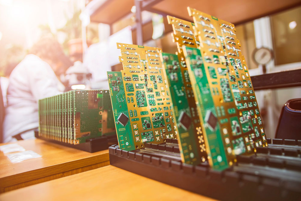
Fig 1: Many Circuit Boards
Most circuit board makers use either of the following three methods.
- Applying iron on the glossy paper technique.
- Also, you can create the circuit by hand on a printed circuit board (PCB).
- Lastly, you can use the Laser cutting edge etching design process.
The latter laser etching process is synonymous with industrial PCB manufacturers.
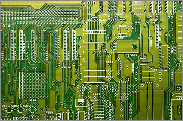
PCB Design

Fig 2: PCB Design in an Electronics Factory
The PCB design procedure involves taking the circuit schematic diagram and imprinting it on a PCB layout. PCB layout software such as Autodesk Eagle or PCBWizard is handy for this procedure.

How to make a circuit board?
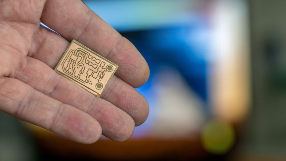
Fig 3: A DIY PCB
Step 1: Prepare the Tools required
- Flat iron
- Photocopying machine or laser printer
- Mini drill
- Eye Goggles
- Latex Gloves
Step 2: Get the Necessary Materials
- A PCB board
- An etching solution, preferably Ferric Chloride (FeCl3)
- A marker- fine tip
- A piece of cloth
- Glossy paper
- Sandpaper
- Plastic straws/ plastic tweezers
Step 3: Design A Circuit Diagram
This step is essential if you don’t have a PCB layout. Alternatively, you may write the simple circuit design on the board if you’re not planning to explore the printing method.
Besides, you’ll need good PCB board design software for an excellent PCB layout design. The Eagle Layout Editor will come in handy in this step.
But if you’re not conversant with this software or looking for a simpler one, go for Microsoft PowerPoint.
Step 4: Draw Your Schematics
We’ll use KiCad for this procedure since it is free and easy to use, even for complex designs. You must install the software and select ‘Create New Project.’
Next, create the circuit diagram schematic and activate the Electrical Rules Checker (ERC). It’s handy for checking for errors in your schematic.
Step 5: Printing Your PCB Layout
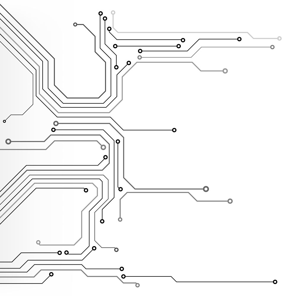
Fig 4: PCB Layout
A laser Printer/ photocopying machine will be handy rather than an Inkjet printer. This is primarily because the latter’s ink is water-soluble.
Hence, it will not transfer its imprint ink on the PCB board.
Again, for this step, use magazine paper or any glossy paper.
Step 6: Cut the Copper Plate for the Circuit Board
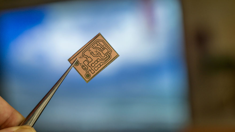
Fig 5: A DIY Printed Circuit Board on Tweezers
Here, it would be best to cut the copper board according to your layout’s size. You may use a hacksaw or a cutter for this task. Next, gently scrub the PCB’s copper side using an abrasive sponge or steel wool to clean the photoresist layer and the oxide covering.
Besides, roughening the surface enables easy image attachment from the glossy paper.
Step 7: Transfer the PCB Print onto the Copper Plate
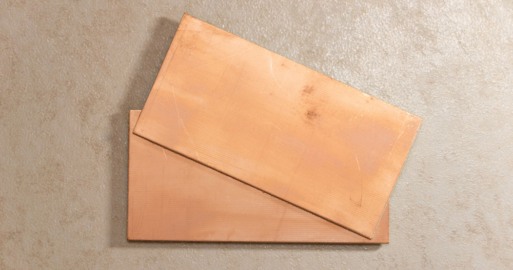
Fig 6: Unused Copper Plates for making Circuit Boards
You may use either of the following two techniques.
Iron on Glossy Paper technique
The method is best suited to complex circuits. Primarily, it involves imposing the laser printer’s image on the board. Besides, ensure that you flip the paper’s top layer horizontally.
Next, place the circuit board’s copper surface on your printed board layout. Also, ensure the board perfectly aligns with the printed layout borders.
A tape will be handy in providing the board and paper remain in the correct position.
Circuit by Hand on PC
Unlike the former method, this best suits simple circuits. In this case, the course will be the reference point from which you’ll make a tracing sketch on the copper plate with a pencil.
Then, after making a clear sketch, use a permanent marker to create a more precise board outline trace.
Step 8: Etch the Plate
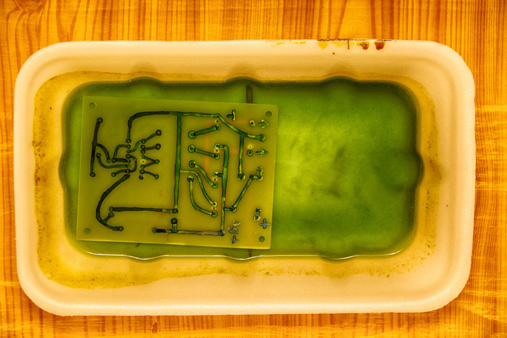
Fig 7: Etching in FeCl3
It is a sensitive step; thus, you must be highly cautious. Here are the key steps and the respective precautions to undertake:
- You should primarily wear rubber gloves and place newspaper on the surface to prevent the etching solution from staining the floor.
- Next, put three spoonfuls of ferric chloride power into a plastic box with water to make the FeCl3 etching solution.
- Now, immerse the PCB in the ferric chloride solution to allow the etching process to begin. The process will prompt the reaction between unmasked copper and FeCl3 to expel unwanted copper from the board. It should take about 30 minutes.
- Using pliers, remove the PCB from the solution and confirm that the unmasked area has undergone complete etching. If not, initiate further etching by dipping it into the solution until the process is entire.
Step 9: Cleaning, Disposal, and the Final Touches for the Circuit Board
The etching solution harms biodiversity; thus, you must discard it cautiously. For instance, don’t pour it into water sources as it’s toxic to water animals like fish.
Also, spewing it into the sink is equally harmful as it could cause drain pipe damage.
Hence, dilute it first with water before discarding it. Also, soak cotton wool with nail polish remover to clean the toner from the plate.
It will aid in exposing the copper surface, and after cleaning, rinse and dry the surface with a clean piece of clothing.
Next, trim the board to your desired final size, and using sandpaper, sand the edges to smoothen it.
Step 10: Drilling the Holes
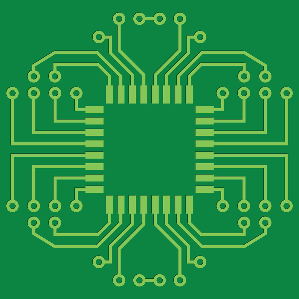
Fig 8: Green PCB
Next, drill holes in the PCB using a hole component and solder the respective components to create integrated circuits.
While drilling, ensure you start from the copper side, as this will guide you to the specific parts to drill.
Note that you can also make a green PCB, which is common in most electronics. All you need to do is smear your board with green solder-resistant paint.
Step 11: How to use a Soldering Iron on a Circuit Board?
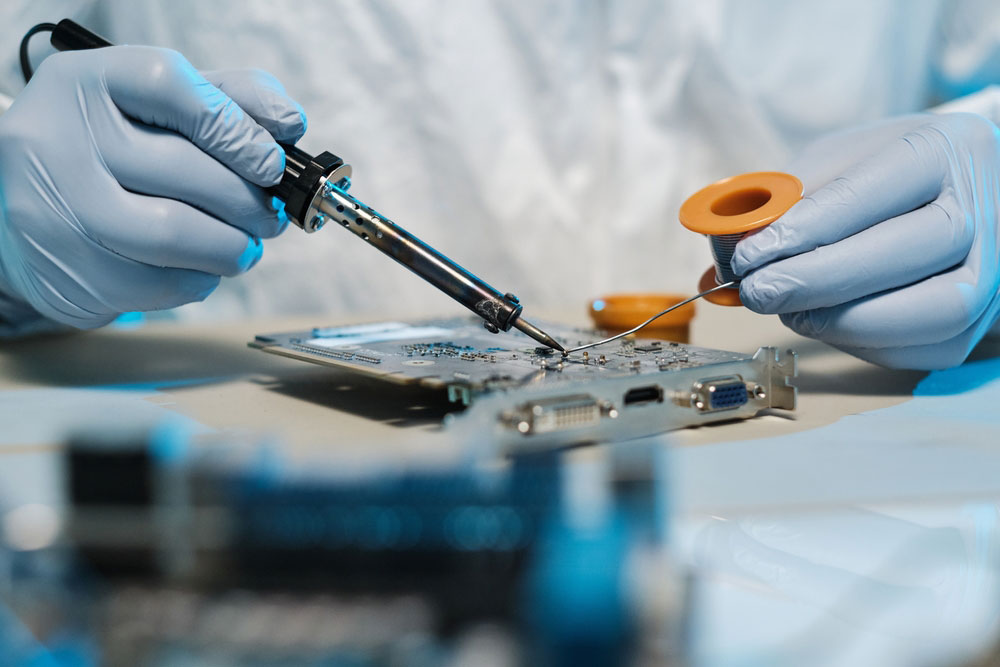
Fig 9: Soldering Components on PCB
Here are the critical stepsforf soldering components onto the circuit board:
How to Build a Circuit Board: Mount the Electronic Component
First, place the component you want to solder by inserting its leads into the circuit board’s holes. Next, flip the circuit board and bend the tips to make a firm connection.
This step prevents the component from falling off during soldering.
How to Build a Circuit Board: Heat the Solder
Switch on the soldering iron and tune it to 400 degrees Celsius. Next, simultaneously place the solder tip onto the copper pad and component lead for about 4 seconds.
This step is handy in heating the pad and melting the information.
How to Build a Circuit Board: Apply Solder
While firmly pressing the soldering iron on the lead and copper pad, place the solder onto the joint. Ensure you don’t directly touch the solder with the soldering iron tip.
When the common you’re making is hot enough, the solder will melt, and a strong connection will form.
Remove the Leads
After soldering:
- Allow the joint to cool naturally.
- Don’t hasten the cooling process by blowing air into the joint.
- Once it’s appropriately cooled, snip the excess lead to remain with a smooth joint.
Noteworthy, don’t apply too much solder to form a large ball connecting to the other joint.
Step 12: Test
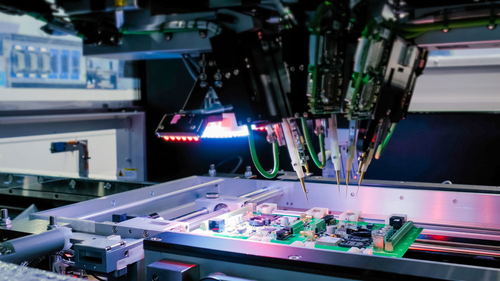
Fig 10: Industrial PCB Testing
Connect the circuit board parts to a multimeter to detect connectivity issues. If present, a desoldering gun will be handy in rectifying the problems.
Conclusion
Now, you’re fully enlightened about how to build a circuit board from scratch.
If you have a query, write to us, and we’ll respond promptly.