Contents
What is BJT Biasing?
Generally speaking, transistor biasing involves applying a specific amount of voltage to a BJT’s base and emitter terminals, improving its efficiency and performance. In this case, the process enables a transistor to amplify an AC input signal in a transistor circuit. So, biasing the BJT will set the emitter-base junction in a forward-biased state. Meanwhile, the base-collector intersection will be configured to a reverse-biased state. Thus, it will operate in the active region.
Also, the collector resistor should have a rating that allows the collector-emitter voltage to exceed 0.5V for germanium transistors and 1V for silicon transistors.
Beta BJT
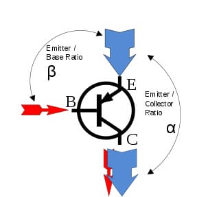
Image showing the current flow process in a bipolar junction transistor.
Source: Wikimedia Commons
Beta (β) refers to the device’s overall sensitivity between the base current and its collector amplification level. It can also identify the device’s gain. For example, a transistor’s base current will amplify by 100 if the β value matches that value. Of course, this factor is generated while the bipolar junction transistor operates in the forward-active state.
BJT Biasing Circuits
We included a few examples of BJT biasing circuits, useful for amplification purposes.
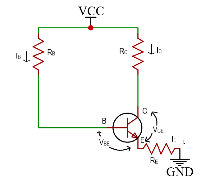
Fixed bias

Fixed bias circuit diagram.
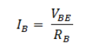
As you can see in the circuit diagram, a base resistor (RB) connects to the VCC and base terminal. In this case, a voltage drop across RB causes the base-emitter junction to set to a forward-biased state. The following formula determines IB’s value.

Both VCC and VBE have a fixed value in the fixed bias type circuit. Meanwhile, RB remains constant. As a result, IB will also have a continuous value, leading to a limited operating point. Thus, this bias type provides poor thermal stability due to its β+1 stability factor.
This occurs due to the unpredictability of the transistor’s β-parameter. It can also widely differ, especially with a similar model and transistor type. The IC will also alter when the β varies. Therefore, this β dependent bias type could experience operating point changes due to the transistor attribute and temperature modifications.
Overall, the fixed base bias circuit relies on minimal components with a simplistic design. By adjusting the RB value in the course, users can change the active region’s operating point. In addition, the source does not have a load since the base-emitter junction features no resistors. As a result, this circuit has switching applications.
The following equations reference the voltage and current for this circuit:

Collector-to-base bias

The circuit diagram represents a collector-to-base bias design.
In this collector-to-base bias setting, two resistors supply the transistor’s active region with DC bias despite β’s value. Since the DC bias comes from the collector voltage (VC), it ensures excellent stability.
Rather than the supply voltage rail (VCC), the base bias resistor (RB) connects to the transistor’s collector (C). An increase in collector current will cause the collector voltage to decrease. In effect, the base drive reduces, decreasing the collector current. This ensures the transistor’s Q-point stays fixed. Thus, the collector feedback biasing technique generates negative feedback surrounding the transistor. That occurs because RB draws direct input from the output, distributing it to the input terminal.
A voltage drop across the load resistor (RL) produces the biasing voltage. So, increasing the load current will result in a significant voltage drop across the load resistor. Meanwhile, it leads to a decreased collector voltage. Afterward, the base current (IB) will drop, reverting IC to its original value.
Dropping the collector current produces a reversed reaction. In that case, this biasing approach refers to self-biasing. Overall, this design provides excellent applications for many amplifier projects.
You can find the circuit equation for collector-to-base bias below:

Fixed bias with emitter resistor
Fixed bias with emitter resistor circuit diagram.
The circuit diagram shows a fixed bias network connected to the transistor’s emitter with an external resistor (RE). Emitter current increases if VBE remains constant as the temperature rises. However, an increased emitter current (IE) causes a boost in the emitter voltage (VE = IERE), leading to a voltage reduction across the base resistor (RB).
The below equation determines the voltage across the base resistor.

Meanwhile, you can determine the base current via the below formula:
This decreases the base current, resulting in reduced collector current since IC matches IB. The formula IC = α IE (α equals 1) defines the collector and emitter current. As a result, this counters the increase in the emitter’s current temperature, ensuring a steady operating point. Replacing the transistor with an alternative type may alter the IC value. Using the same technique as above will nullify any changes, keeping a persistent operating point. Therefore, this biasing network provides improved support over the fixed base bias network.
Overall, the circuit utilizes this equation:

Voltage divider bias or potential divider
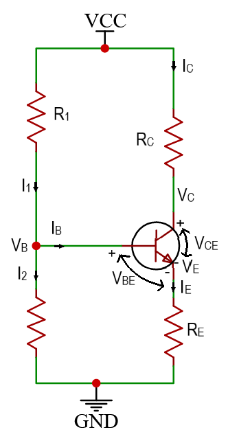
Voltage divider circuit diagram.
As you can see, two external resistors, R1 and R2, integrate into this circuit to create a voltage divider. This setup allows voltage generated across R2 to set the transistor’s emitter junction to a forward bias state. Overall, the current flowing through R2 will be ten times higher than the necessary base current.
Generally, this biasing type means that variations occurring in VBE and β will not affect IC, which, in turn, provides maximum thermal stability. A temperature increase will cause IC and IE to boost. This results in a higher emitter voltage, resulting in a lower base-emitter voltage. Afterward, this leads to a decrease in base current (IB), reverting IC to its initial state.
Regardless of the decreased amplifier gain, this biasing circuit has popular applications due to its maximized stability.
The circuit relies on the below formula:

Emitter bias
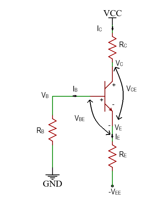
Circuit diagram showing an emitter bias design.
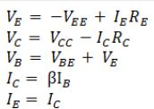
The circuit, as shown above, relies on two power supply sources, VCC and VEE, to operate. These feature matching but opposite polarities. VEE sets the base-emitter junction to a forward-biased state. Meanwhile, VCC forms the collector-base intersection to a reverse bias state.
Additionally, IC can rely on RE >> RB/β and VEE >> VBE rather than VBE and β. Doing so provides a balanced operating point.
Summary
As you can see, BJT biasing ensures that the transistor will operate correctly in a circuit, providing AC signal amplification. It achieves this by selecting resistors that affect the transistor’s operating point. Additionally, the collector junction sets to a reverse bias state while the emitter-base sets to a forward-biased state. Of course, the circuit design will depend entirely on the intended application and what you want to achieve.
Do you have any questions regarding BJT biasing? Feel free to contact us!