Contents
What is a CD4013?
CD4013 dual D flip flop is an IC chip. It uses clock pulses to reset the output data to high or low.
CD4013 Pin Configuration

CD4013 pinout
The table gives the details on IC pinout as per the CD4013 datasheet.

How To Use The CD4013
Using a CD4013 is simple as long as you follow the proper steps.
- First, connect the ground/ GND pin to the negative supply terminal and the VDD pin to the positive supply terminal.
- Then, to provide the required voltage, check the exact values of the chip in its datasheet. Often, the power supply voltage ranges from 3V to 15V. However, other CD4013 versions can support up to 20V of the maximum supply voltage.
- The data (D) pin receives the input data stored in the flip-flop.
- Providing a signal on the CLK pin (low to high) helps keep data to output pinQ from pinD.
Note: The opposite of pin Q is output pin Q1.
- Finally, the reset(R) pin forces the output pin to be low, whereas the set(S) pin forces the IC to be high.
CD4013 Alternatives
You will often find some alternatives to 4013 IC with extra characters at the end, for example, CD4013BE. Other examples include HEF4013, TC4013, HCF4013, MC14013, and NTE4013.
Additionally, you can use the CD4013 ICs with the following D flip-flops;
- 74HC9 and 74H74 – Dual D-type flip-flop.
- 40175 and 4175 – Quad D-type flip-flop.
- 4174 and 40174 – Hex D-type flip-flop.
CD4013 Example Circuit
Coin Tosser
The application circuit of CD4013 IC we’re going to illustrate involves a coin tosser.

A Coin Tosser circuit using CD4013 IC
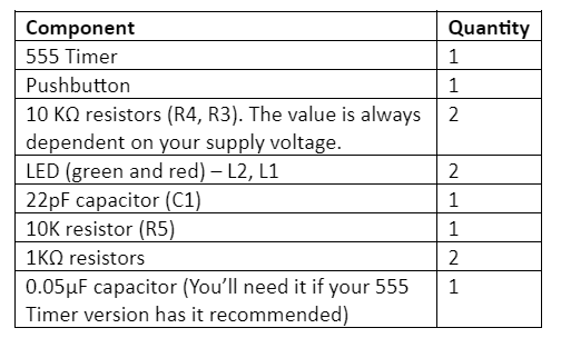
Components needed
Circuit explanation
The guide below summarizes the working of a coin tosser circuit with CD4013.
- First, after pushing the S1 button, the 555 timer creates a fast-switching clock signal to the CD4013.
- Then, the D input will receive an inverted output from the IC flip-flop. In other words, the flip-flop IC changes to the opposite of its initial state after every clock pulse. Therefore, if there’s a continuous clock signal supplied to the IC, it will toggle between low and high.
- L2 symbolizes tails, while L1 symbolizes the heads of a coin, and only one LED will simultaneously remain lit. One has a connection to the inverted output, as the other connects to the normal output.
- R2 (1000Ω), R1 (1000Ω), and C1 (22pF) use the 555 timer IC to set the clock frequency. When generating approximately 20 clock pulses per second, you can use the values stated.
- R5 operates as a pull-down resistor that ensures pin4 of the 555 timers is low with no pushed button. Ultimately, the 555 timer stays reset and doesn’t send clock pulses. R5 can have a value ranging from 10k to 100k Ω.
Conclusion
Generally, CD4013 is a bare CMOS chip with two Data/ D-type flip-flops. We have gone through its application, operation, and other necessary information. If, however, you have questions or need clarifications, kindly contact us.