Contents
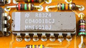
1. What is CD4066?
CD4066 is a CMOS IC with four switches belonging to the family of CD4000 ICs. It falls under the category of analog switches.
One of the CD4000 series
Source; Wikipedia
The 4-bilateral switch design of CD4066 is mainly for transmitting analog or digital signals and multiplexing.
2. Pin configuration
CD4066 quad bilateral switch is a 14-pin IC. We’ll discuss the functionality of each pin below.
- Pins 1, 3, 8, and 11 – They are input pins for the 4-bilateral switches.
- Pins 10, 9, 4, and 2 – They are the output pins for the quad bilateral switches.
- Pins 13, 12, 6, and 5 – They are the control pins for CD4066.
- VCC (pin14) – It’s the power source to the Integrated Circuit.
- Ground (pin7) – it’s the ground pin of the IC.
3. Features
The specifications and features of CD4066 are as follows;
- First, they have a low internal resistance of 5 ohms and an on-state resistance of 5Ω.
- The Maximum voltage of the control pin at low levels is 0.9V, whereas its minimum voltage at high levels is 11V.
- Also, the packages of CD4066 are often 14-pin PDIP, PDSO, GDIP/DIP14, SO14, or TSSOP14. In addition, the chips each have four channels.
- Besides having high linearity, it also has a high on/off o/p voltage ratio and a control i/p impedance.
- Then, the noise immunity is 0.45 VDD, and it also has a peak-to-peak analog switching of ±7.5V.
- Then, its operating temperature ranges from -55°C to 125°C.
- It has an operating voltage ranging from 3V to 18V and a maximum voltage for switching of 20V.
- Moreover, it has a bandwidth of 40 MHz and a 1:1 SPST configuration.

SPST symbol
Source; Wikipedia
● It has less crosstalk amidst the four switches of -50Db with an RL of 1kΩ.
● Finally, it has a high output current of 0.4mA and a low off-state switch leakage.
Note: CD4066 and CD4016 are very similar in their pin configurations. However, you’ll find a distinguishing feature in the internal resistance. CD4016 has a resistance of 200Ω, while the resistance in CD4066 is 5Ω. For that reason, CD4066Ω mostly suits weak signal applications like audio signals.

4. Where can you use CD4066 Quad Bilateral Switch?
Often, you’ll find in CD4066 quad bilateral switch multiplexing applications and in isolating signals. And since it’s bilateral, you can use it in both analog and digital signals.
Furthermore, other than the normal operating voltage range of 3V to 18V, you can also use 15V, 10V, or 5V nominal voltages. And it can get to a peak voltage of 20V.
An advantage of the 4-channel switch over a single-channel switch IC is constant ON impedance over the input voltage range. Additionally, the voltage of the peak input is similar to the complete power supply voltage.
5. How to use CD4066 Quad Bilateral
CD4066 analog switch operates via four switch signals (often analog) via a digital control. So, after applying the input analog signal to the switch, it’ll proceed to the control terminal input. Then, you get an output signal.
CD4066 is a bilateral switch. Therefore, it can work in reverse and forward directions.
- So, each switch has two pins, that is, the output pin and the input pin, carrying out voltage switching.
- Pin14 has a connection to the +ve terminal, while pin7 is at the ground terminal in the circuit.
- If you have a control input of 1, the switch terminals develop a low impedance, causing a switched-on state. Contrarily, a switch input of 0 will shut off the switches, and the switch terminals will have high impedance.
Let us consider a single switch circuit diagram that uses CD4066 IC for better comprehension.
Electronic components required
- CD4066 switch IC,
- A Direct Current motor, and
- A battery source – 12V of power supply.
We’ve connected the DC motor in series with our switch IC. Then, the 12V supplies the required energy needed to run the motor. Further, depending on the switch IC range, you’ll have a varying voltage range of 5V to 18V.
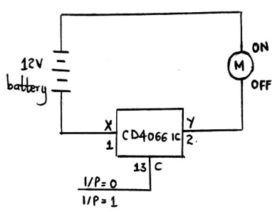
Single circuit diagram using CD4066 IC
Circuit operation
After simulating the circuit, we notice that with a lack of control signal, the motor stops operating. But, on placing a high logic control signal at the switch’s control pin, the motor switches on and begins rotating.
We can conclude that the switch’s function is to use a power signal to modify the control signal. As such, it can work as a switched multiplexer.
CD4066 4×1 Multiplexer
In our second application, we’ll use a four-by-one multiplexer CD4066 IC. It has a single output and four selection lines (i.e., control pins). Then, in designing your circuit using the multiplexer IC, you’ll have to connect all output pins to a common point.
To better comprehend our explanation, check the circuit diagram below;
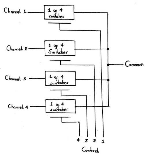
CD4066 Multiplexer circuit
6. Applications
You can find CD4066 quad bilateral in a wide range of applications like;
- Dead-band filter,
- Sample and Hold (S&H) circuits,
- Conversion of digital-to-analogs or analog-to-digital signals,
- The 4-input multiplexer in electronic systems,
- Analog-signal gain, phase impedance, and digital control of frequency,
- In the implementation of logic transmission gates,
- Squelch control,
- CMOS logic implementation,
- Modulators, demodulators, choppers, commutating switches,
- Network switching,
- Multiplexing and switching of digital and analog signals,
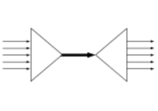
Multiplexing process
Source; Wikipedia
● Sample and hold circuits.
Conclusion
Briefly, CD4066 is a 4-bilateral switch with four inbuilt switches that you control discretely with a control pin. Its bilateral feature is that it can conduct in both forward and backward directions as a multiplexer switch.
Finally, if you have any questions or clarifications, kindly contact us.