PCBs are electrical components that act as building blocks in an electrical circuit and electronic devices. Some examples of PCBs can include highly complex high-speed circuit boards, multilayer boards, flexible circuit boards, etc.
Then, we have another term linked to PCBs, i.e., a circuit trace. PCB traces are systems and hence need uttermost precision and design to function sufficiently, as we’ll see in today’s article.
Contents
What is Circuit Trace?
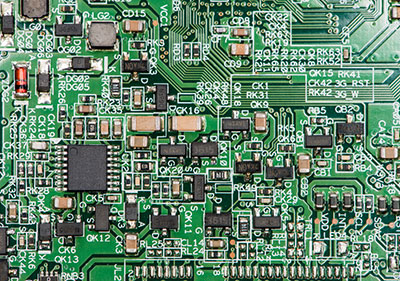
A circuit trace is a network of conducting tracks like fuses, copper layers, and insulation that electrically connects PCB components. When there’s an inconsistent circuit board trace, an electronic device, particularly its circuit path, will malfunction.
Circuit electric trace
Source; Pixabay
Further, it ensures the electric current flow has little to no trace resistance. Resistance in some applications often results in heat dissipation hence damaging the components. When there’s no electrical resistance, heat flow occurs from areas of higher temperature to lower temperature areas.
Circuit Trace Thickness
Have you ever wondered why an electronic designer highly regards the thickness of circuit traces?
The trace thickness maintains a PCB balance, which contributes to better board functionality. Failure to take into account the trace thickness can bring some board challenges.
Trace thickness differs with the type of PCB board. For example, there is a multilayered, double-sided, and single-sided board. In addition, the thickness will depend on the PCB version in use.
Lastly, most PCBs have a range of trace thickness starting from 0.008 to 0.240inches.

Examples of Trace thickness levels
PCB Trace Current/Capacitance
A direct current acts as the power source of PCBs. In other words, electrical current flows through the board wiring and copper layer while electrons directly go to the battery. Circuit tracing differs from a trace current in that PCB traces display how conductors and wiring interact to produce current.
Then, always consider a PCB trace current because, without it, you won’t generate any power. Also, use conductors and insulators to make specific electric currents calculations (measured in Amperes). However, ensure you don’t supersede the required PCB power since it might cause a short circuit.

How to Compute PCB Trace Spacing?
Knowing the PCB trace width or spacing parameter is crucial in its PCB design. For instance, ensure you have enough trace width to prevent damages like overheating when transferring an expected quantity of current.
Types of online calculators
Generally, we have two online calculators that help gauge the trace width. They include IPC 2221 and 2152, developed by the Association of Connecting Electronics Industries (ACEI). They are the standard calculators used in commercial and industrial applications.
At first, the trade association introduced IPC 2221 calculator. Unfortunately, it lacked several parameters like board material and board thickness and, therefore, wasn’t perfect for trace width calculations.
Later on, after several studies and experiments, ACEI released a more efficient calculator, IPC 2152, in 2009. It had added parameters like;
- distinctions amid external and internal traces,
- plane’s location,
- heat sink,
- board thickness,
- working on multilayer PCBs.
Calculating the Trace width
Undeniably, calculating PCB width traces isn’t easy. Thus, you can use a trace width table to calculate faster. Also, you can use an online calculator for calculations.
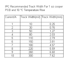
IPC recommended track width for 1 oz copper PCB and 10°C temperature rise
Aspects that you should consider to get a precise calculation include;
The maximum current limit your PCB can handle. The limit aspect considers several factors like trace’s ambient temperature, measurement, trace temperature, and trace thickness.
Then, after adding numbers to your calculator, you’ll get the results. Normally, the trace width figures comprise;
- trace resistance measured in ohms,
- voltage reduction measured in volts,
- power dissipation in watts,
- width in amps, and
- trace temperature measured in Celsius.
Later on, collect the input details from the PCB datasheet or physical PCB. Since circuit boards are compact, you might need a lens to get the input info.
The details are on the circuit display. Thus, you won’t engage in guesswork. Furthermore, the calculator doesn’t make any calculations when it receives unprecise measurements or numbers.
Now, you can use the formula below to start your calculations;
I=k*ΔT^0.44*A^0.725
Whereby;
I’ = PCB trace current (always constant).
ΔT = temperature change.
A = Cross-sectional area of PCB trace.
As for the width, first, get the current’s cross-sectional area to pass through safely, then use the formula below;
Area [mils^2] = Current/ Temp_Rise [deg. C]) ^ 0.44)) ^ (1/0.725)
Next, find the PCB trace thickness for width calculation.
Width[mils] = Area[mils^2]/(Thickness[oz]*1.378[mils/oz])
Note;
Designers often consider the formula above as industry standard and thus accurate. Be cautious when carrying out the project since the formulae may not automatically fit every design.
How to Cut PCB Trace?
You’ll need a knife, PCB-scraper, milling tool, and screwdriver to break/cut a PCB trace, provided they have a sharp edge.
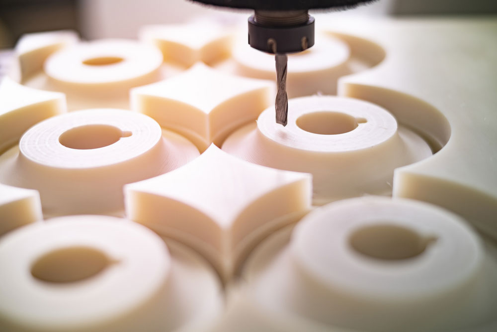
(milling machine)
First, carefully scratch or scrap the PCB trace in a back-and-forth manner.
Afterward, remove the thin layer of copper traces accurately and slowly. It ensures you incur no damage to the surrounding traces while performing the task. Also, the corner of a screwdriver can scratch the trace when vertically cutting it.
Conclusion
All in all, PCBs make up most of our array of applications in electronics. For that reason, it is essential to know about printed circuit traces for your PCB longevity.
We hope that the post has enlightened you on circuit tracing. Please feel free to contact us if you need clarifications or have questions.


