Contents
What Is The DMOS Transistor?
The DMOS FET is an acronym for the Double diffusion metal oxide semiconductor field-effect transistor. This transistor is among the family of RF Power N-channel MOSFET transistors.
This commercial power MOSFETs’ name comes from the manner of sequence in which the transistor operates.
This electrical device operates by first diffusing the p-doped substrate. Then, subsequently following, it up with the highly doped n+ source diffusion.
This activity helps maintain the power levels in a double-diffused bipolar transistor.
Also, the Double-Diffused MOSFET works by using the Bipolar-CMOS-DMOS (BCD) automation for astute integrated circuits.
Additionally, its physical structure helps with the double diffusion activity, which is perfect for audio power amplifiers.
Hence, it is a common power semiconductor device. The drift region and p region are the main workers in the diffusion process. In addition, the design of power MOSFETs has its p region with more depth.
This particular semiconductor material is a commonly used transistor. The popularity is due to its ability to bridge all the hindrances of the uncontaminated bipolar IC.
Notably, some of the limitations include reducing the amount of power dissipation since it lacks the current driving requirement.
Also, it efficiently works in fast-switching applications when you apply the correct amount of base current.
(transistors.)
Importantly, the length of the channel, breakdown voltage control, and access resistance are vital features of this semiconductor material.
These factors are important because the two dopant impurities possess different lateral diffusion speeds.
The lateral diffusion rate assists in deciding the channel length and helps with the load power supply.
Also, these dopant impurities have an additional implantation dose. Additionally, the dopant impurities access the DMOS FET through an opening in the polysilicon layer.
This feature gives this power device structure a short channel length from the lithographic step in the user process.
Notably, there are numerous layouts of the DMOS transistor. However, the layouts majorly depend on the range of voltage and peak power that operates the transistor.
Therefore, you can use the DMOS transistor in amusement, industrial, and office equipment.
Also, you can use it in air conditioners, vending machines, and water heaters.
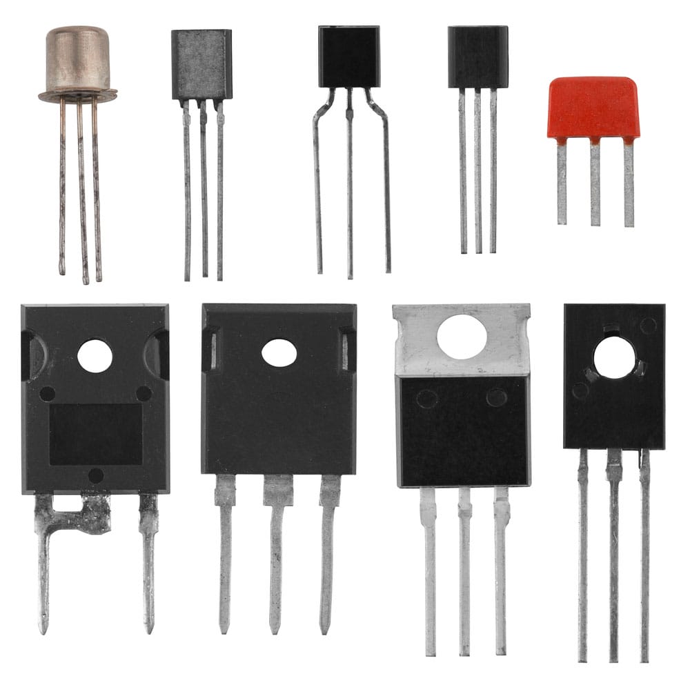
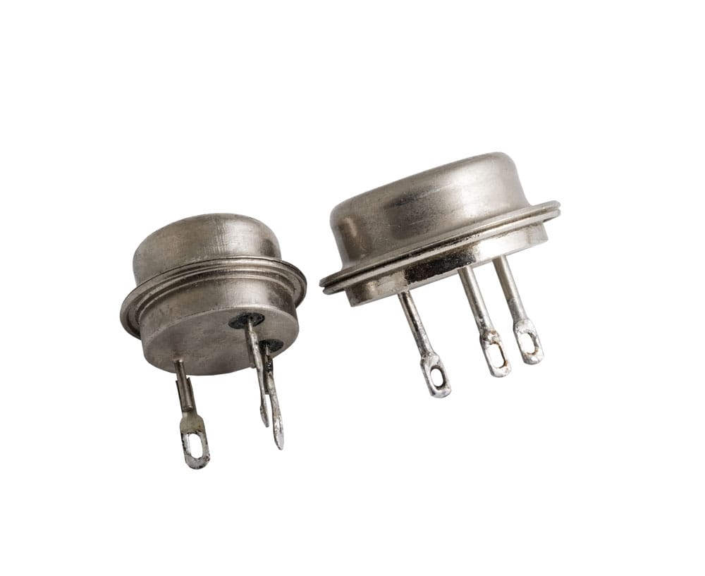
(transistors on a white background)
Double-Diffused MOS (DMOS) Structure
The double-diffused MOS (DMOS) physical structure comprises silicon dioxide, a silicon substrate, warm oxidation, polycrystalline silicon, and a semiconductor.
The power circuit’s current ratings are altered due to the electricity that infiltrates it.
Also, the holes with positive charges can undergo basic doping from the amalgamate surrounding the gate electrodes and the semiconductor.
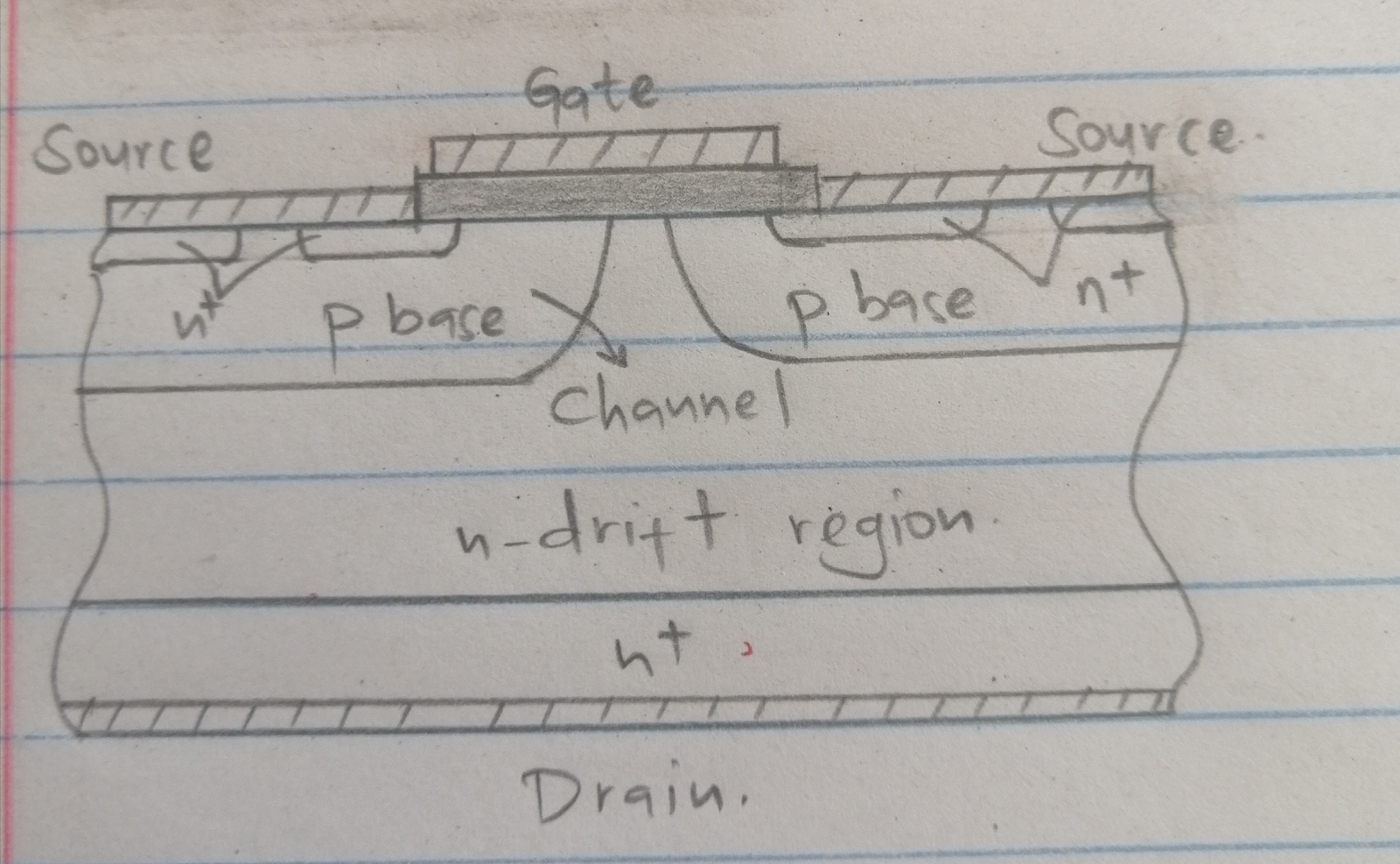
(Diagram of the DMOS Structure)
Explanation
The junction termination extension produced by the n+ and the p-type diffusions underneath the gate oxide controls the channel length.
The basic structure channel length can also be the lateral dimensions between the p-n substrate junction and the n+ p-junction.
Notably, this channel dimension can be about 0.5mm long.
First, when the operation voltage increases towards the gate electrodes, electrons pass through the transistor.
The electrons then move from the p region to the n region. Next, an electrical connection via the metal oxide flicks the inversion layer of the p-substrate region on and off.
This process happens due to the command of the gate voltage. Notably, the position of the gate is between the source terminal(p region) and the drain terminal (n region).
Finally, the electrons (carriers) depart after a trip through the n region.
Importantly, you should know that the n-type substance has a low doping level.
Therefore, there is enough space to consider the expansion of the depletion layer between the source and drain terminals.
Further, this property results in a higher breakdown voltage between the drain and source terminals.
The drain to source voltage depletion FET has undergone several developments.
Consequently, the device has become one of the major power field-effect transistors.
However, the initial DMOS device was very big because of its lateral structures and drain inductance. This feature resulted in the device’s advantages being offset.
As a result, the design and development of the vertical extension of the vertical structure began.
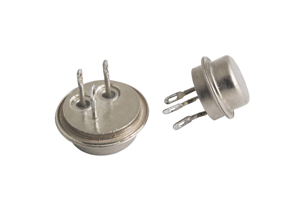
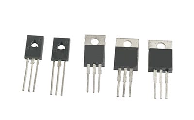
(picture of power transistors.)
What Can DMOS Transistors Do?
Below are some of the attributes of the Double-diffusion MOS transistor.
- Firstly, this power electronic has an overly high current density with corresponding breakdown voltage ratings. Therefore, you can achieve this property from the low doping level in the region between the drain and channel regions.
- Secondly, the DMOS is quite similar to the Bipolar Junction Transistor. Notably, the similarity is due to the high base current, breakdown voltage characteristics, and high frequency.
- Thirdly, voltage depletion FET can switch the speed up a mega swift in high-frequency power cycles without detecting power loss.
- Also, the field-effect transistor can accommodate conductive connection signals of the wideband type. Importantly, this property causes the capacitance and on-state resistance to subside and maintain low charge injection.
- Moreover, the p region semiconductor layer has additional impurities implanted within semiconductor regions, ensuring proper punch control. Also, the threshold voltage drop doesn’t get out of hand, and that is due to the light doping level in the drift region. Consequently, the velocity saturation passes and the drain region is the identical twin of the drift region.
- Next, you utilize the entire transistor arrays in DMOS transistors to finish the good electrical connection process.
- Moreover, these high-voltage MOSFETs provide energy efficiency compared to a low-voltage transistor. Power devices need proper energy efficiency for them to function.
- Lastly, they can work on the low and high sides depending on the task and charge carriers.
(a silhouette of a bipolar junction transistor.)
What Is the Difference Between CMOS and DMOS?
Complementary metal-oxide-semiconductor(CMOS) is among the types of semiconductor devices. The MOSFET has a power consumption without a high static current and oxide capacitance.
Also, the MOSFET produces a small amount of waste heat and channel resistance that remains quite high. Moreover, the power usage is kept down, which is a plus.
The CMOS works with transistor arrays to construct memory chips, image sensors, and other digital circuits.
Also, the CMOS is about an intricate set of methods that seamlessly gel well with product transistors.
The CMOS utilizes output voltage when it is under a conductive connection. Consequently, the intricacy level of the circuit can control voltage.
Contrastingly, the DMOS uses a heavy flow of power and has a drain current that controls the drain voltage.
You mainly use the device as a high and fast frequency switch. Also, the make-up of the device is from oxidation and various silicon.
The Double diffusion process needs the gate, body, source, and drain. Moreover, it handles the electric current accumulation without needing a detectable electric current.
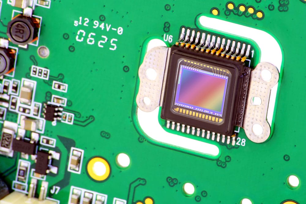
(CMOS sensor from a camera.)
Summary
The DMOS transistor is a structure that employs double diffusion with the p region and n region as the leads. Importantly, the DMOS transistors are crucial in circuit-making, and they are energy-efficient.
Also, the DMOS and CMOS are very revolutionary since they hugely assist the tech world.
We hope this article is of great help to you.
Please reach out to us for more information on this article or any circuits.