Does your electronics project require impedance matching? Or do you need a circuit with a transistor that can pull a little current from the input? In other words, you need an introductory course that can offer current and power gain. Well, if this relates to your situation, you’re in the right place. And the ideal amplifier circuit for handling the issue mentioned above is the emitter follower circuit.
And the best part is:
We’ll take you through a comprehensive breakdown of how the emitter follower works. Also, you’ll see details on how to build the circuit, its applications, and more.
Let’s begin!
Contents
What is an Emitter Follower Circuit?
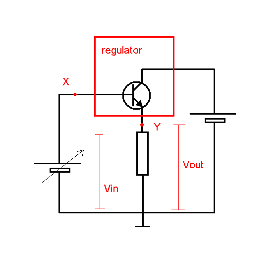
Emitter Follower Regulator
Source: Wikimedia Commons
The emitter follower is the network you get from using an emitter terminal as output in a BJT configuration. Also, this configuration’s input base signal is usually a shade higher than the output voltage. And this happens because of the inherent base to emitter drop.
So, you can say that the emitter load in this type of single transistor circuit follows the transistor’s base voltage. And it does this in a way that the emitter terminal’s output is always equivalent to the base voltage minus the base-emitter junction’s forward drop.
Usually, when you connect the BJT to the zero supply rail, the base will need about 0.7V or 0.6V. And it requires the voltage to complete switching of the device within its collector to emitter. Hence, this transistor’s operational mode is the standard emitter mode.
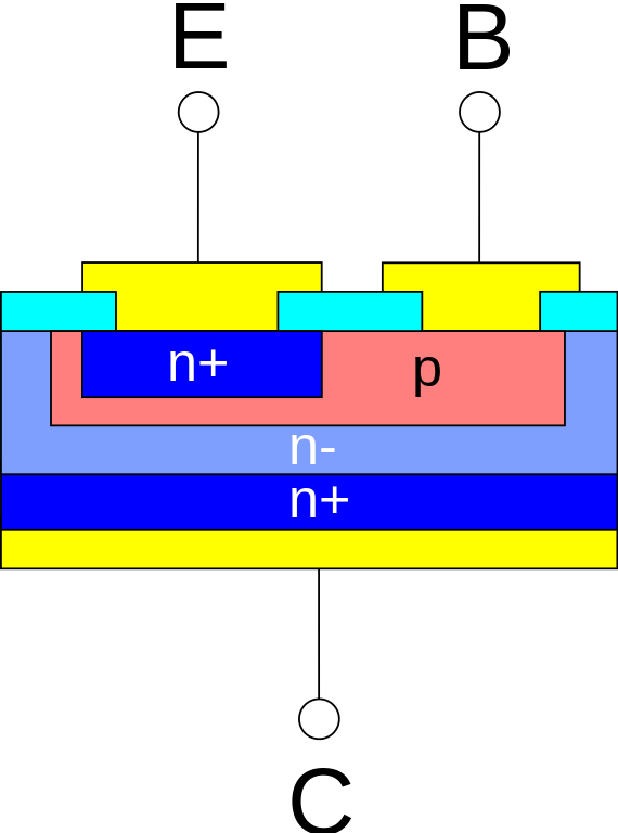
NPN structure Bipolar Junction Transistor
Source: Wikimedia Commons
Also, the 0.6 or 0.7 V value is the BJT’s forward voltage value. Interestingly, the load in this configuration always connects to the device’s collector terminal.
In addition, it also means that the device will be optimally saturated, forward biased, or turned on. But this only applies as long as the BJT’s base voltage is 0.6V higher than the emitter voltage.
The Key Features of the Emitter Follower Transistor
- The collector current sources are equal to the emitter current. Consequently, the configuration is usually rich in current—if you connect the collector directly with the positive supply rail.
- When you connect the load between the ground and emitter, the base won’t have a high impedance. And it also means that the base circuit has protection from high wide range current. So, it doesn’t need high resistance for protection. Plus, the base terminal isn’t vulnerable to connect to the ground rail via the emitter.
- The emitter voltage will change when you vary the base-emitter junction voltage.
What is the Working Principle of the Emitter Follower circuit?

Emitter Follower Diagram
Source: Wikimedia Commons
Typically, a suitable emitter follower circuit has a voltage gain of about one, i.e., Av @ 1. But, when it comes to the collector voltage response, the emitter voltage is usually in-phase with the input base signal (Vi).
So, it means that the output and input signals will instantaneously reproduce their positive and negative peak levels. Also, you’ll notice that the Vo (output signal level) will follow the Vi input signal level. And it does this via an in-phase relationship that depicts its name “emitter follower.”
Hence, the emitter-follower configuration has a low impedance at the output and high impedance features at the input. And you can use the format for impedance matching. Further, this feature is the opposite of a fixed-bias input circuit configuration.
How Do You Make an Emitter Follower Circuit?
Emitter Follower Circuit Diagram
Source: Wikimedia Commons
Before you build an emitter follower circuit, you need to consider factors. For instance, you need to consider the current passing through the transistor. Also, the AC signals’ frequency cutoff goes into the input and the DC voltage supplying your transistor’s collector.
That said, here are the components you need for the circuit:
- Wires
- Load Resistor
- Resistor (3.3KΩ)
- A power supply that has outputs +15V, -15V, and ground
- NPN transistor (2N3904)
- Sagging voltage source
Steps
Step 1
Refer to the emitter follower circuit. While you’re at it, do the following:
- Position your transistor properly. Then, connect your collector to +15V. And ensure that you confirm your transistor’s documentation because the pin orders can be different.
- Link your emitter to -15V with your 3.3KΩ resistor.
- Move to your transistor’s base and connect your sagging signal.
- Then, fix your load to the transistor’s emitter.
Step 2
It’s vital to provide the correct range of voltages to the NPN transistor’s collector and the base. Hence, if you put a voltage signal at the transistor’s floor, the transistor will permit load current flow. Consequently, the internal current flow of the transistor will adjust until the following happens:
- The voltage at your base should be 0.6V higher than the emitter’s voltage.
- Most current (about 99%) comes from the collector. So, only about 1% of the current that leaves the emitter comes from the base.
So, the first condition explains why the emitter follower’s output signal follows the input.
The second condition gives a breakdown of how an emitter-follower lessens sag. That is, the emitter-follower can supply the load with a large amount of current. In the process, it draws some current from a sagging voltage signal.
And this is possible because only 1% of the emitter current comes from the base. Also, for a similar load impedance current draw, the voltage source will only sag a small amount (1/100). In other words, the emitter-follower reduces the voltage source’s Thevenin Resistance by a factor of 100.
Step 3
If, for some reason, your transistor in an emitter-follower can’t modify to meet the conditions above, you have to do clipping. That said, the pair of transistors can adjust only when the output voltage sends current to the circuit’s right side. And when the current supply comes from the transistor, it will boost the output voltage (VOUT). The increase will continue until the base voltage is 0.6V less.
But you have to remember that the current can only move out of the transistor’s emitter. And there’s no way the transistor can lessen the VOUT without entirely cutting the wind. So, when the current leaves the transistor, a voltage divider will remain. And the voltage divider has two resistors (3.3KΩ). Both resistors lie between -15V and ground.
At this stage, the voltage divider will adjust the output voltage to 7.5V. And the signal will clip at -7.5V since the transistor can’t decrease the VOUT below the baseline.
That said, you’ll notice the clipping at the signal’s top. After all, the transistor only allows the current to move from the collector to the emitter. Plus, it can’t output an emitter’s voltage that’s bigger than the collector’s voltage.
Further, the output can’t exceed +15V irrespective of the input signal. So, clipping will occur.

What’s the Difference Between CE and Emitter Follower Circuit?
| Common Emitter | Emitter Follower Circuit |
| It’s a simple device that helps you to create voltage gain. | This device is effective as a voltage buffer. And it helps to drive loads. |
| When you take the output from the common emitter, it gets a gain of nearly two. | When you take the emitter follower circuit’s output, the signals become close to in-phase with each other. And the gain is almost one. |
Applications
You can use an emitter follower circuit for the following applications:
- Antenna tuners
- Acoustic horns
- Baluns
- Simple motor speed controller
- Hi-Fi power amplifier
- Simple variable power supply
- Signal generator circuit
Rounding Up
You can use the emitter follower circuit in many applications. And it’s because the course has a low output impedance and high input impedance. Also, the system is perfect for impedance matching.
That said, it’s pretty easy to set up the emitter-follower circuit. All you need to do is understand the constructional details and follow the steps explained in the article.
Do you need help with constructing your circuit? Or do you want to get the best emitter follower circuit for your project? Please feel free to reach us.