Think of a scenario where you want to obtain an opposite logic-level voltage output. Such an outcome is only possible if you run the input voltage through an inverter. Specifically, this article focuses on the Hex Inverter circuit and the wide range of functions of this sort of IC.
Contents
What is a Hex Inverter?
Figure 1: Industrial Inverters
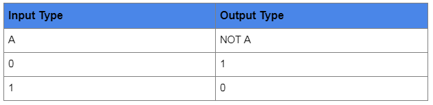
The role of the inverter ICs is to reverse the applied input signal. Hence, a Hex inverter Integrated circuit represents types of Inverter ICs featuring up to six inverter circuits. Also, applying a low input voltage to the inverter produces a high output voltage and vice versa.
Hence, by performing these functions, the NOT gate/ inverter acts as a basic logic gate capable of logical functions such as negation. The truth table below explains how the logic families of inverters work:
Hex Inverter IC: 74HCT04
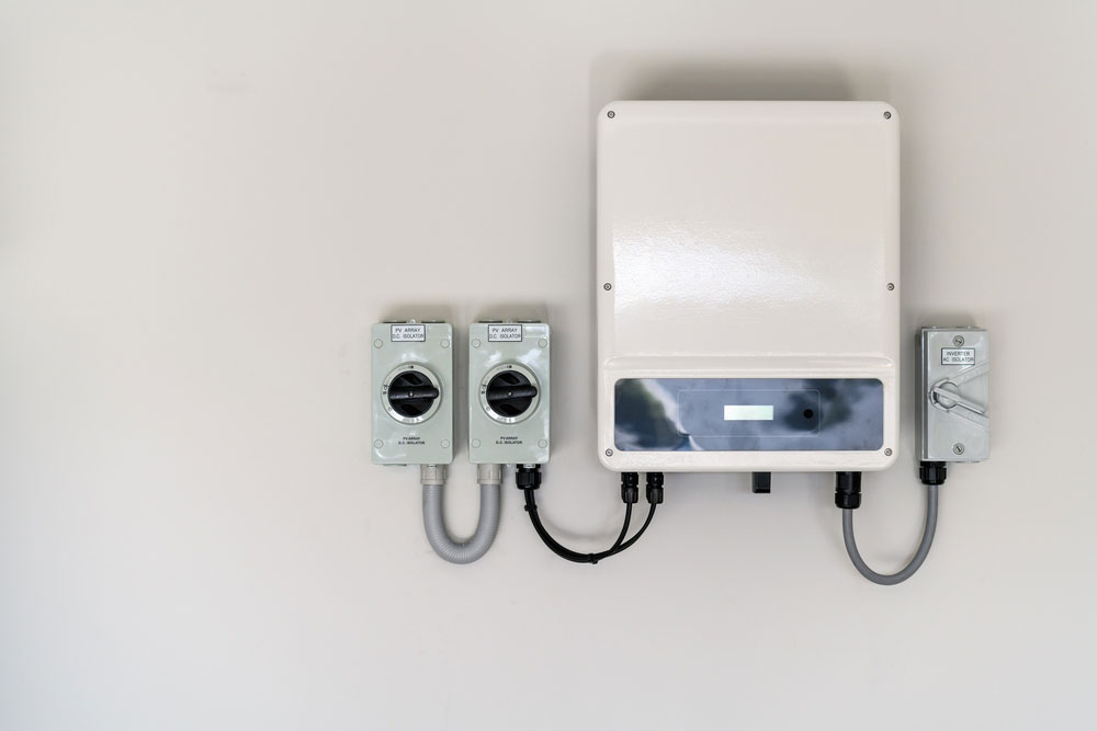
Figure 2: New solar panel inverter with isolators attached to the wall
Meaning
Digital devices with 74HCT04 ICs feature up to six self-sustaining inverters. Each of the trigger inverters has a push and pull output. Also, the IC sports low-powered Schottky on its pins.
The fundamental aim of the protection is shielding the IC’s input pins from damage by excess input Vcc. Therefore, it further has current restraining resistors to enable the protection functionality.
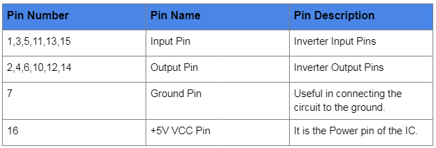
Pin Configuration
The table below gives the respective functions of the input and the output pins of the IC.
Note: Every chip of the 74HCT04 features NOT Gates.
Features
- The module (6-self standing inverters) is RoHS compliant, Lead-free, and available in SO- 14 and TSSOP -14 packages.
- Also, its voltage range is between 4.5V – 5.5V, and it has a continuous output current of +25Ma.
- Thirdly, it has a minimum level of high input voltage and maximum input low-level voltage of 2V and 0.8V, respectively.
- Besides, its TTL-compatible pins have a transition time of 29 ns and feature a Schmitt trigger on its input pins.
How to Use 74HCT04 IC
All the NOT gates in the IC have their respective input and output pins. Thus, during use, connect the power supply to the IC’s pin 16. Also, you need to connect pin 8 to the ground, and you’re good to go.
Circuit Diagram
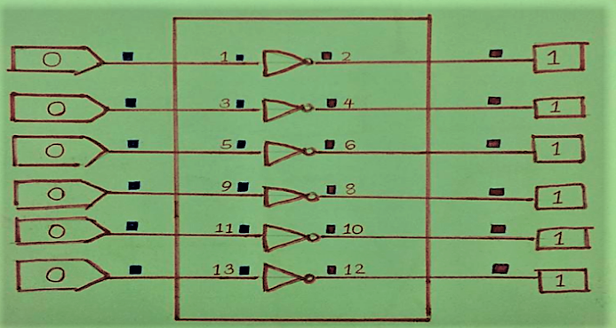
Figure 3: Circuit Diagram
74HCT04 inverter circuit Propagation delay
The IC can operate as a wave oscillator/ buffer. But, you must take the switching time/propagation delay into account to realize this function. Essentially, this is the duration the output pin will take to switch the input type of signal to the other form.
This module’s propagation delay duration is 29-nanosecond. Thus, it’s ideal for various applications, such as the generation of clock signals, buffering, and a square wave generator.

Hex Inverter IC: 4049 IC
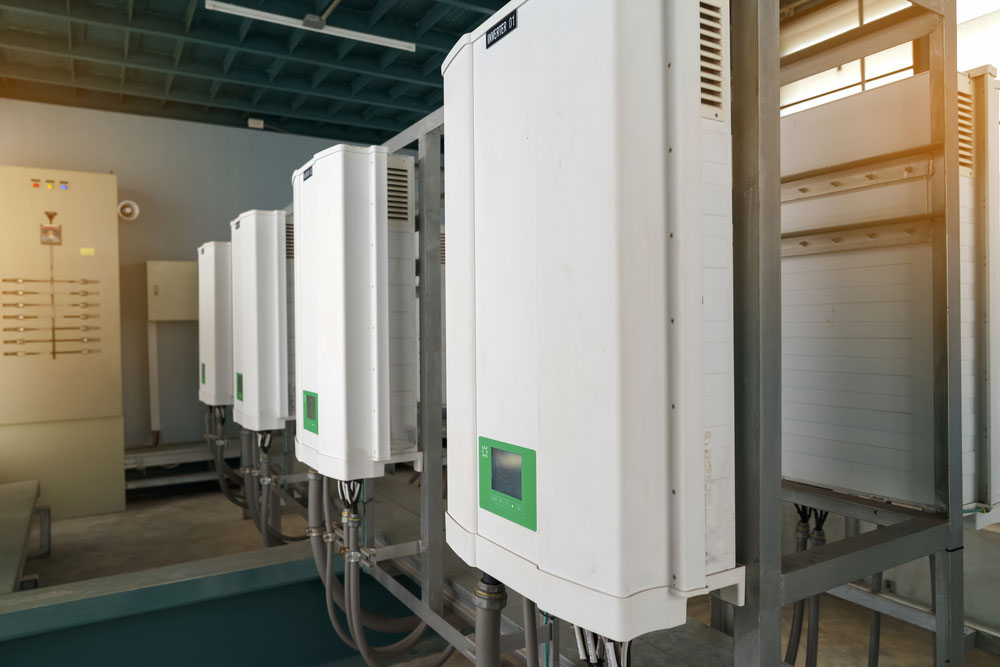
Figure 4: Industrial electricity Inverters
Meaning
As the IC mentioned above, it is also a six NOT gates inverter buffer that is specifically useful in CMOS TTL converters. Also, you’re likely to find it in DTL converters type of devices.
In addition, it can operate not only Transistor-Transistor Logic but also Diode-Transistor Logic.
Pin Configuration
- It is a 16-pin module with each other pins having the following respective functions.
- Pin 1 is the level input voltage pin.
- Next, Pins 2, 4,6, 10, 12, and 15 are the inverting o/p pins for i/p 1, 2,3,4,5, and 6, respectively.
- Then, Pins 3, 5,7,9, and 11 are the Input Pins 1,2,3,4 and 5, respectively.
- Pin 8 is the VSS pin or the negative supply pin of the IC.
- Lastly, Pins 13 and 16 are the NC (Not Connected) Pins.
Features
- The IC is common in voltage multiplier circuits and enables max input voltage supply.
- Also, it’s a Hex Inverting Buffer kind of logic function with a variety of packages, including TSSOP, SOIC, SO, and PDIP.
- Thirdly, the module’s maximum sink currents can drive up to two TTL loads.
- Other features include; an ambient temperature of between -40 and +85°C, a maximum supply current of 50mA, and a 22.5pf max input capacitance.
How to Use 4049 IC
The module is commonplace in 12-24volts voltage doubler circuits. Also, in regard to functionality, 4049 integrated circuits are similar to rectifier circuits. Nonetheless, unlike rectifiers, voltage doubler circuits not only change DC to AC but also step up DC voltage. Hence, these circuits are handy where high DC voltages are required.
Circuit Diagram
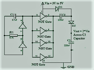
Figure 5: Circuit Diagram
Applications
The IC is useful in the following areas:
- CMOS HEX Converters
- Source Drivers
- Voltage multiplier circuit
- o/p reversing
- CMOS conversion to DTL/TTL
Hex Inverter IC: CD4069
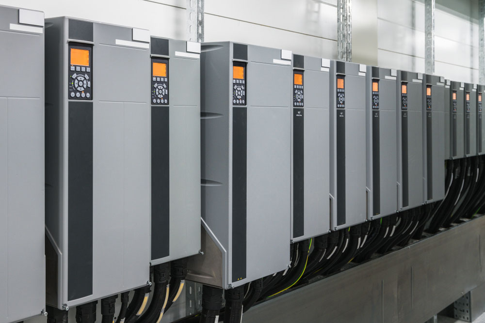
Figure 6: Variable speed drive inverter converters
Meaning
In terms of working principle, the CD4069 is similar to the 74HCT04 we covered above. Thus, both ICs are capable of noise immunity.
Pinout.
The Pin configuration of the IC is also similar to that of the 4049 IC. Nonetheless, it is noteworthy that the CD4069 features MOSFET P and N structure which make up an inverter gate logic.
Circuit Diagram
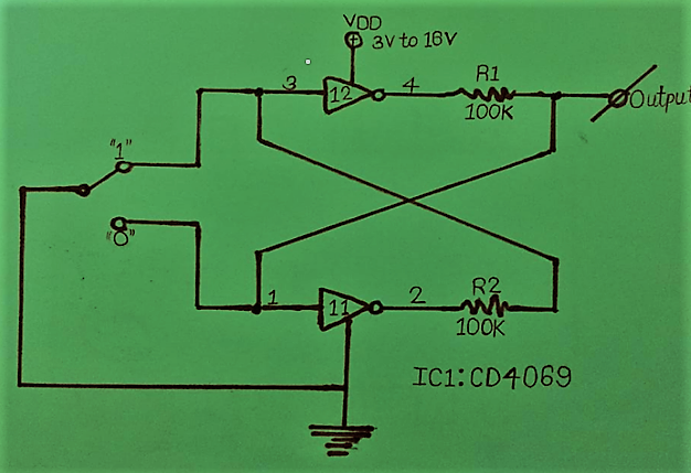
Figure 7: Circuit Diagram
Applications
The module is essential for uses such as the following:
- Enabling logic reversal and pulse framing
- Manufacture of oscillators and high input impedance amplifiers.
Conclusion
In summary, this article should help you understand the working principle and pinout of most Hex inverter ICs. Thanks for your time, and in case you have any queries, talk with us at any time, and we’ll respond immediately.