Contents
What exactly is IGBT?
IGBT stands for Insulated Gate Bipolar Transistor. It’s a 3-terminal semiconductor electric device that provides fast switching capabilities at high efficiency.
To better understand an IGBT, it’s best to understand different transistors in terms of functionality.

Transistors
A transistor is a small electronic component with two main functions. It acts as a switch to control lighting circuits and can amplify signals.
There are different types of transistors based on other usefulness or specific applicability. The commonly used transistors are BJT (Bipolar Junction Transistor), MOSFETs, and IGBT.
Both BJTs and MOSFETs have their preferences, as well as advantages over the other. While BJTs prefer low on-state drops, MOSFETs are best for their high I/P impedance, low switching loss, and lack of secondary breakdown.
The IGBT combines both the BJT and MOSFET, whereby it takes the best of both transistors.
Therefore, an IGBT is a three-terminal device used as a switching device and applicable in amplifying signals. IGBT provides fast switching at high efficiency.
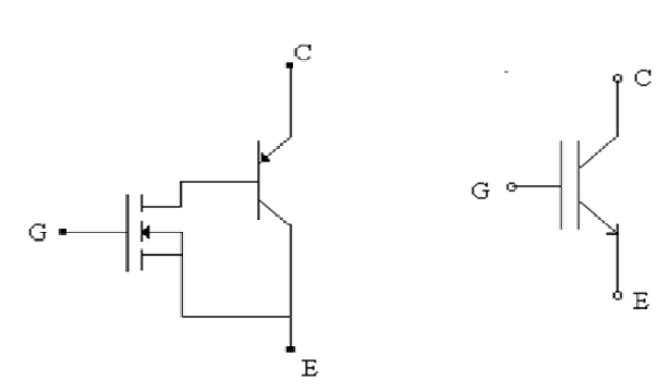
IGBT Symbol
Since IGBT combines BJT and MOSFET, its symbols follow the same principle as below.

IGBT Symbol
The symbol also has three terminals – the Collector, Emitter, and Gate. The input side represents the MOSFET, while it takes the output symbol from BJT’s symbol.
As expected, the conduction terminals are the Collector and Emitter. The Gate is the control terminal.
Structure of IGBT
All three terminals (Collector, Emitter, and Gate) of IGBT are attached with metal layers. However, the metallic material on the Gate terminal has insulation of a silicon dioxide layer.
Internally, the IGBT structure is a four-layer device of semiconductors. The four-layer device comes about by combining PNP and NPN transistors, which make up a PNPN arrangement.
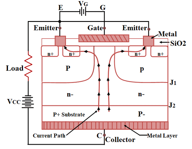
Structure of IGBT
Source: Components101
The layer closest to the Collector region is the (p+) substrate, the Injection Region. Right above it is the N- NDrift region, which comprises the N- N-layer.
The Injection Active Region injects most of the carrier (the hole current) from the (p+) into the N- layer.
The thickness of the Drift Region determines the voltage-blocking capability of the IGBT.
On top of the Drift Region is the Body Region, which consists of (p) substrate. It is close to the Emitter. Inside the Body Region, there are (n+) layers.
Note that the junctions between the Collector region (or Injection Region) and the N-Drift Region are J2. Similarly, the junction between the N- NRegion and the Body Region is junction J1.
NOTE: IGBT’s structure is topologically similar to a thyristor in terms of the “MOS ” gate. However, the thyristor actions and functionality are suppressible, meaning that only transistor action is permissible in the IGBT’s entire device operation range.
The IGBT is preferable over the thyristor because of the fast toggling over the thyristor’s wait for zero crossings.
How Does an IGBT Work?
The IGBT working principle is ON or OFF by either activating or deactivating its Gate terminal.
If a positive input voltage goes across the Gate, the Emitter keeps the drive circuit ON. On the other hand, if IGBT’s Gate terminal is zero voltage or slightly negative, it shuts OFF the circuit application.
Since the Insulated Gate Bipolar device both functions as a BJT and MOSFET, the amount of amplification it achieves is the ratio between its output and control input signals.
For a conventional BJT, the amount of gain is approximately the same as the ratio of the output current to the input current. We referred to it as Beta and denoted it as β.
On the other hand, for a MOSFET, there is no input current because the Gate terminal is an isolation of the main channel carrying current. We determine the IGBTs gain by dividing the output current change by the input voltage change. This makes the IGBT a trans-conductance device.
Operation of IGBT as a Circuit
Let’s explain this using the figure below, which describes the IGBT’s entire device operation range.

Operation of IGBT as a Circuit
The IGBT only works if there is a supply of voltage on the Gate terminal. It is the Gate Voltage, which is VG.
As seen on the diagram, once there’s a Gate Voltage (VG), the Gate Current (IG) increases. It then increases the Gate-Emitter Voltage (VGE).
Consequently, the Gate-Emitter voltage increases the Collector Current (IC). Thereby, the Collector Current (IC) decreases the Collector-to-Emitter Voltage (VCE).
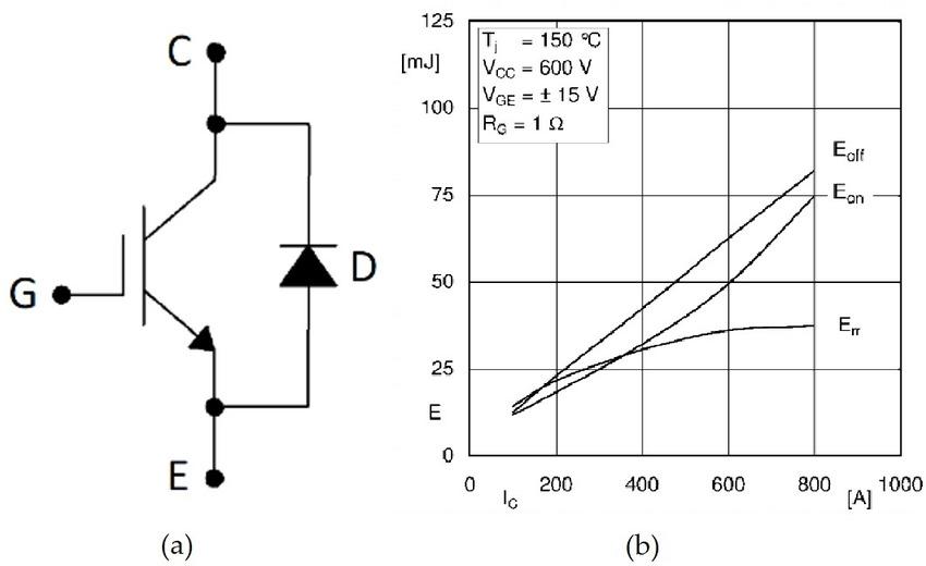
NOTE: The IGBT features a voltage drop similar to diodes, typical to the order of 2V, which only increases with the current’s log.
The IGBT uses free-wheeling diodes to conduct reverse current. The freewheeling diodes are placed across the device’s Collector-Emitter terminals.
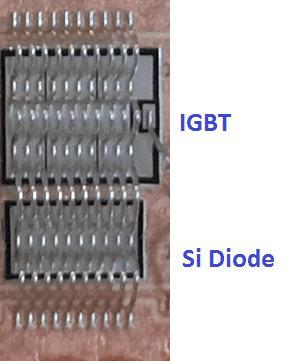
IGBT, Si Diode
Source: Researchgate Publication
The in-built diode is a requirement on IGBTs because the power electronic device can fail the power switch without it. Since switching OFF, an inductive load current generates high voltage peaks whenever there’s no suitable path.
IGBT and FWD module
Source: Researchgate
Whenever the Insulated Gate Bipolar Transistor turns off, the minority carriers from the N- Region flow out to the external circuitry. After the depletion layer expands (Collector-Emitter Voltage rises), the minority carriers cause internal recombination of current flow, the tail current.

Types of IGBT
As a four-layer device, IGBTs are classifiable based on the presence of the (n+) buffer layer. Insulated Gate Bipolar Transistors with the (n+) buffer layer are the Punch through IGBT (or simply PT-IGBT).
Similarly, IGBTs without the (n+) buffer layer are the Non-Punch through IGBT (or simply NPT-IGBT). Here’s a table of their differences.

Insulated Gate Bipolar Transistors are further classifiable on their characteristics. The device design concept for PT-IGBT and the NPT-IGBT can be either symmetrical or asymmetrical.
The symmetrical IGBTs have equal forward and reverse breakdown voltage. At the same time, asymmetrical Insulated Gate Bipolar Transistors have their forward breakdown voltage greater than the reverse breakdown voltage.
This means that symmetrical IGBT is mainly applicable in AC circuits. On the other hand, asymmetrical IGBT is applicable in DC circuits, and that’s because they don’t need any supported reverse voltage.
IGBT Models
Circuits using the IGBT working principle usually feature modeling using circuit simulators like Saber and SPICE.
The simulators can model the IGBT (and other actual devices) to provide the best predictions regarding currents and voltages on the electrical terminals.
For an even more precise prediction, heat and temperature are included in the simulation process. The most common modeling methods for IGBT’s device design concept are:
- Physics-based model
- MacroModel
The SPICE simulator uses the MacroModel method, which combines various components, such as MOSFETs and BJTs, using a Darlington configuration.
IGBT Working Principle– Electrical Characteristics
Due to IGBT’s reliance on voltage to function, the devices require only a tiny amount of voltage supplied on the Gate terminal to maintain conduction.

Electrical Characteristics
It is the opposite of Bipolar Power Transistors, which need a continuous Base current flow at the Base region to maintain saturation.
At the same time, the IGBT is a unidirectional device, which means it only switches in a “forward direction” (from the Collector to Emitter).
It is the opposite of MOSFETs, which have a bi-directional current switching process. In practical devices, MOSFETs are controllable in a forward direction and uncontrolled in reverse voltage.
Note that under dynamic conditions, the IGBT may experience a latch-up current when the device switches OFF. When a continuous ON-state driving current seems to exceed a critical value, this is a latch-up current.
Also, when the Gate-Emitter voltage goes below the threshold voltage, a small leakage current flows through the device.
At this time, the Collector-Emitter voltage is almost equal to the supply voltage. Therefore, the four-layer device IGBT is operating in the cutoff region.
IGBT Working Principle–Applications of IGBT
The IGBT is usable in small-signal amplifiers, just like MOSFETs and BJTs. However, the IGBT makes the best of both, thus features low conduction loss and high switching speed.
IGBTs uses are in most modern electronic devices, such as stereo systems, trains, VSFs, electric cars, air conditioners, etc.
IGBT vs. MOSFET
Insulated Gate Bipolar Transistors are best in high voltage, low switching frequencies, high current configurations.
Conversely, MOSFETs are best in low voltage, high switching frequencies, and medium-current domains.
IGBT vs. MOSFET
Source: Researchgate
The IGBT is usable on practical devices with switching frequencies lower than 20 kHz due to its high switching loss.
Summary
We hope you now understand what IGBTs are and how they differ from MOSFETs and BJTs.
Do you have questions or concerns about the IGBT?
Feel free to contact us!