Contents
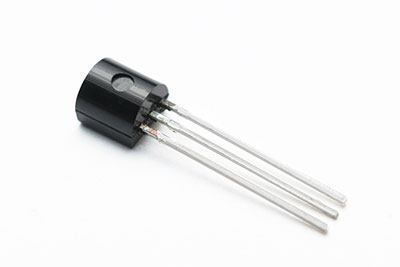
J111 JFET Pin Configuration
J111 JFET has three pins in its pinout. They comprise gate, drain, and source pins.
- Pin1/ Drain terminal – It allows current flow into the chip.
- Pin2/ Source terminal – It controls JFET biasing.
- Pin3/ Gate terminal – It connects to GND and is an output of current from the chip.
Feature
The features and maximum ratings of J111 JFET include the following;
Note: Maximum ratings are individual stress limit values that determine the amount of damage the j111 can withstand.
- It has an internet N0132S geometry with high input impedance.
- Then, it is RoHS compliant.
- Its operating and storage junction temperature ranges from -65°C to +150°C, whereas it has a lead temperature of 300°C.
- Also, it has a high-power gain – 1 5mS typical, and low noise – 1.2 nV/√Hz Typical.
- Its power dissipation is approximately 625mW.
- Further, both the maximum gate-source voltage and maximum drain gate voltage are 35V.
- Lastly, it’s available in TH (through-hole package), Bare Die, and SMT package options. It also includes package type TO-92 pin count and a surface mount SOT-23 package.

How Does JFET Work?
We will use two working scenarios to explain how a JFET works;
First Case
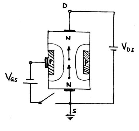
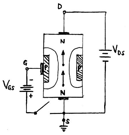
First circuit illustration on JFET’s working
It begins by applying voltage VDS between the source and drain terminals with no gate voltage. Consequently, you’ll gain depletion layers established by the two p-n junctions in the bar sides.
Then, the flow of electrons from the source to the drain terminal through the channel formed between the depletion layers will start.
Note: Depletion layers’ sizes determine the current conducted via the bar and the channel width.
Second Case
A second illustration of how JFET works
Here, we’ll work in reverse. Therefore, we’ll apply VGS voltage between the source and gate terminals. With the supply, we’ll increase the width of the depletion layer.
Subsequently, the conducting channel will reduce and increase the resistance of the n-bar, therefore decreasing the source to drain current.
Contrarily, decreasing the gate’s reverse bias decreases the width of the depletion layer. Afterward, the current from the source to the drain rises due to an augmented width of the conducting channel.
Please note that n-channel and p-channel JFETS have a similar operation. The only difference is that p-channel JFETS use holes and not electrons as carriers of channel current. Moreover, they have reversed VGS and VDS polarities.
Equivalent of J111
As an equivalent or replacement of J111 N-channel JFET, you can consider J107. It is a cost-effective switch operating as a low-noise JFET amplifier.
(electronic JFETs)
- The difference between JFET and BJT
Bipolar Junction Transistor and JFET have differences as per the table;
| JFET | BJT |
| It uses the base current to control the wind between the emitter and the collector. | It is a bipolar transistor since both holes and electrons aid in conduction. |
| Its input circuit has reverse biasing, therefore contributing to a high input impedance. | The forward biasing in its input circuit results in low input impedance. |
| JFET is a unipolar transistor because it has one carrier type, i.e., electrons in the n-type and holes in the p-type channel. | The presence of junctions results in an increased noise level. |
| It uses the base current to control the wind between the emitter and the collector. | It uses gate terminal voltage to regulate the current between the source and drain. |
| Here, the gate terminal doesn’t receive current. | On the other hand, BJT receives a few µA base currents. |
J111 JFET Application
J111 JFET is common in high gain and low noise applications, as listed below.
- Choppers,
- Audio and industrial applications,
- Analog switches, and
- Commutators.
Conclusion
To conclude, J111 is a JFET chopper transistor that functions on many supply voltages. Furthermore, its operating parameters make it a suitable product for many technical experts because it’s straightforward.
That’s all for today. However, for further inquiries, do not hesitate to contact us.