Contents
1. Several Experiences of PCB Traces
- The first lines at the end of input and output should be avoided adjacent parallel to avoid reflection interference. Ground wire isolation when necessary. The wiring of the two adjacent layers needs to be perpendicular to each other.
- Second, analog to digital has a short circuit; please note that there is only one connection point, and there is no common on the PCB, which is determined by the system design.
- Third, the distance between standard components is 100mil(2.54mm). So the grid system’s base is generally defined as 100mil (2.54 mm) or less than the integer multiples of 100mil. Like:50mil、25mil、20mil, etc. Generally, the layout 50mil of the grid, 5mil of wiring, a distance of holes, and the device is 25mil (so that the device can wiring between the lines)
- The PCB board delay is 0.167ns/inch. The delay will be increased if many holes, device pins, and a multi-constrained cable set.
- The wider the wire diameter is, the closer the power is, or the higher the dielectric constant of the isolation layer is, the characteristic impedance is smaller.
- Wiring on PCB is equivalent to the capacitor in series and parallel. Parallel resistance is usually very high. Any high speed and high power consumption of the device should be placed to reduce the supply voltage transient overshoot.
- If you are using CMOS or TTL circuit design, the wiring length should be less than 7 inches when the operating frequency is less than 10MHz, at 50MHz shall be no more than 1.5 inches, while if the frequency reaches or more than 75MHz, the length should be 1 inch.
2. Several Methods of PCB Wiring

2.1. Right Angled Wiring
This way usually is avoided in wiring, which is also a standard to measure wiring quality. Because it will make changes to the width of the transmission
2.2. Differential Wiring
The differential signal is widely used in high-speed circuit design. Compared with the ordinary single-ended signal, the differential signal has obvious advantages:
First of all strong anti-interference ability, effective suppression of EMI, and accurate timing positioning.
Secondly, for PCB engineers, the biggest concern is how to ensure that it can fully play the different wirings of these advantages in the actual layout. These rules are not used to move rigidly; many engineers seem not to understand the nature of high-speed differential signal transmission.
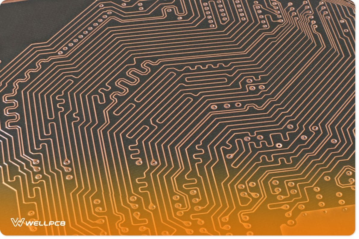
2.3. Serpentine Wiring
It is the most common use in wiring layout. The main purpose is to adjust the delay and meet the system timing design requirements. But it will destroy the signal quality, and change the transmission delay, the wiring should be avoided as far as possible.