Contents
1. In the electronic printed circuit boards (PCBs) a lot of capacitors are found.
The quantity and value of capacitors become higher as the switching frequency of the IC rises. On the other hand value of the capacitors in the power supplies varies inversely so that their value decreases as the frequency of pulsating DC (ripples) increases.
2. The ICs degrade their output performance if there is any type of ripple noise.
This noise effect is more apparent in the analog ICs as compared to the digital ICs. All ICs require a certain level of power supply regulation which is a small fraction of the required power supply mentioned in their datasheets. The power supply requirements and noise margins are becoming more and more stringent as the requirements of ICs are becoming low.

3. A decoupling capacitor
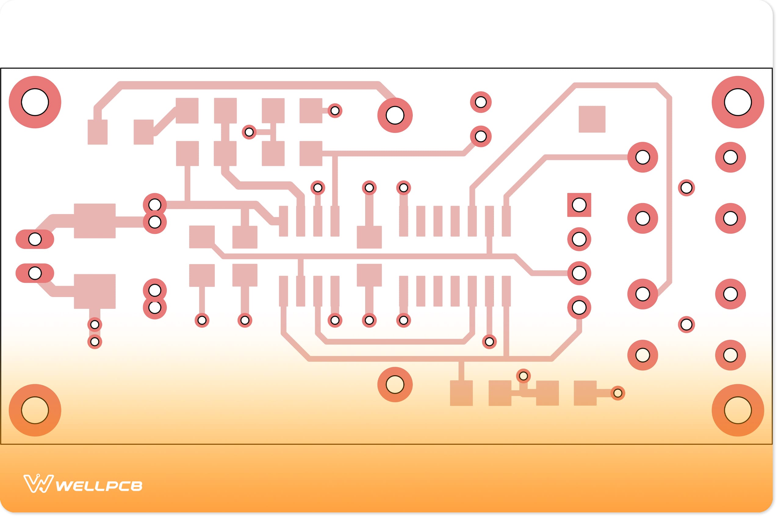
An ordinary capacitor placed very close to the supply pin of the component suppresses ripple noise from the DC power supply and fulfills the instantaneous current requirements of an IC. It removes very tiny ripples from power supplies that are already smoothed and regulated. They also act as an instantaneous power supply backup source for an IC when the voltage drops down due to IC switching. It is a common practice to place a network of decoupling capacitors, i.e. a combination of different high values (hundreds of µF), medium values (a few tens of µF), and low-value capacitors (a fraction of µF), as shown in figure
1. This practice is effective for circuits where the noise of multiple frequencies is apparent. This occurs in the voltage levels due to power supply regulation, length of power cables, PCB and wire parasitic, switching frequencies EMI effects, etc. The most commonly used values for small decoupling capacitors are 100nF, 220nF, and 470nF. They are connected to the IC power pin (such as ±5V, 3.3V), connecting one side to the power supply pin and the other side to the circuit current returns (ground). They are placed as close as possible to the pin but not compromising on the minimum components to component clearance, as shown in Figure 2.
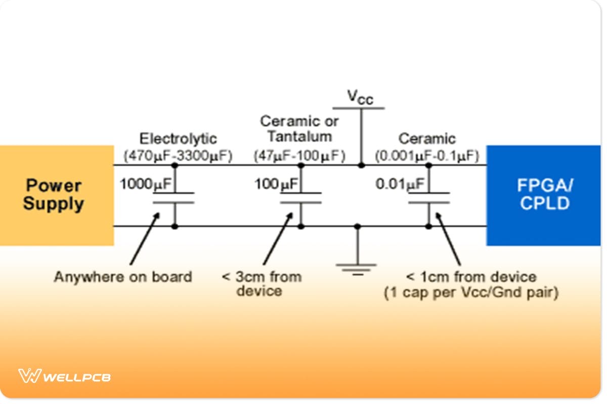
Figure 1: Decoupling capacitors network schematics
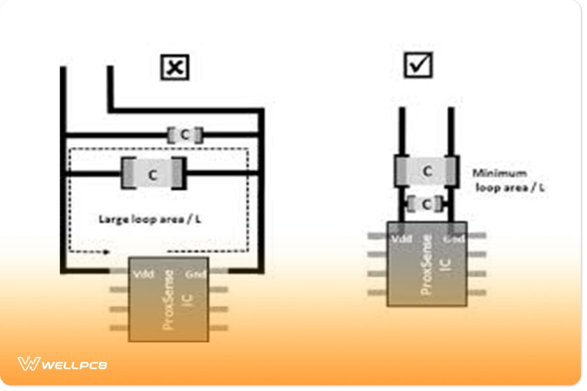
Figure 2: Decoupling capacitors placement