Contents
1. 3D PCB Printers


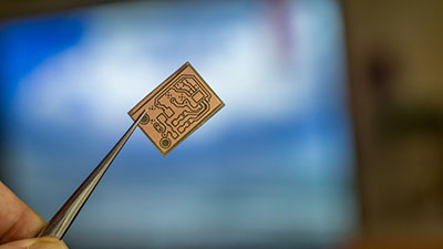
2. Flexible PCBs Making and Wearable Technology
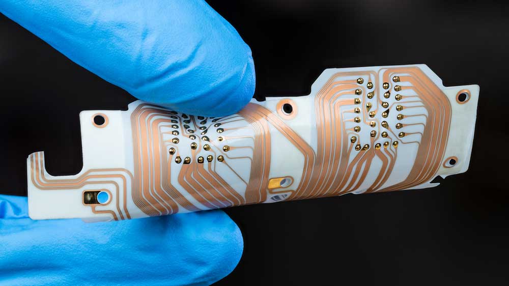
There has been an increase in the need to bring electronics closer and closer to our bodies. This is mainly due to health reasons. It is becoming more and more important to monitor human health now. And then rather than waiting for a normal doctor checkup or waiting until you feel sick. Flexible PCB (FPCB) has come in handy to leverage wearable technology. The use of traditional rigid printed circuit board Making in wearable technology is getting minimized day after day. The copper tracks are now being built up, and they are being made thinner and thinner. This makes wearables more comfortable to put on and more efficient in operation, especially where the wearable sensors’ data is transmitted wirelessly.
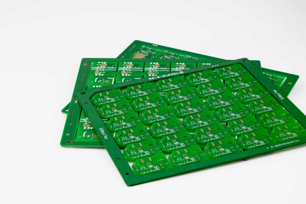
3. High-Density Interconnects PCBs (HDI PCBs)
There is an obvious need for miniaturization. Whether you want to make a board for a wearable application, a new computer board, or just an Internet of Things (IoT) device, electronics components must be tiny to occupy so, the smallest space with superior performance in printed HDI technology, PCB components can be packed very close to each other and function even better. With microvias, which are about 140um, components can be densely packed to as close as 100um. However, this is achieved without compromising the quality of the electrical signals involved.