The new and improved Integrated Circuit Op Amplifier 741 is fast making its way in the Àtechnological field. Apart from offering circuit flexibility in analog circuits, it has come a long way in its application in analog computers. With several pins in place i.e., 8 in total, IC Op-Amp 741 carries out its function effectively while depending on the exterior feedback for regulation. What is more, its application in electronic circuits and devices renders it suitable and safe.
To learn more about the importance of this amplifier on its mechanism of action, specifications, and applications, continue reading.
Contents
1. What is the Op Amplifier 741?
Generally, an operational amplifier, also known as an Op-Amp, is a high voltage gaining (approx. 100dB) solid-state integrated circuit. Its design is primarily recommendable for executing analog computations. That is to say, its role is to perform mathematical operations such as integration, subtraction, differentiation, addition, among others.
Further, combined with external components, for instance, capacitors and resistors, to produce a mandatory feedback mechanism, you can use it as an amplifier. Also, you could transform it into a comparator or filter.
Undoubtedly, there is a variety of Op-Amp ICs making up the vital components of analog circuitry. However, we will specifically dwell on the commonly used Op-amp, the IC 741 Op Amp.
Definition on IC 741 Op amp
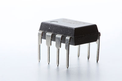
An IC 741 op-amp comprises the general-purpose Op-Amp circuit but with an outstanding feature of a monolithic chip in the integrated circuit.
Fairchild semiconductors had the first manufacture of an op-amp 741 in 1963. Since then, 741 has been an indicator of this operational amplifier whereby it has one output pin, four input-taking pins, and seven functional pins.
Characteristics of a 741 Op-Amp
The integrated circuit Op-Amp has the following characteristics;
- First, a voltage gain of about 200000.
- Then, a frequency range of the amplifier signaling is from 0Hz to 1MHz.
- Also, the o/p is below 100 ohms.
- Input impedance above 100 kilo-ohms.
- Finally, low offset voltage and input offset current.
2. Specifications of IC 741 Op-Amp
Some of its basic specifications are:
- Power supply: It can handle a voltage of 5V, while the maximum can go up to 18V
- Output impedance: Approximately 75Ω.
- Input impedance: Approximately 300 KΩ to 2MΩ (megaohms)
- Voltage gain: Can be 20000 to 200000in cases of low frequencies (20 or 200V/Mv)
- The maximum output current: About mA.
- The input offset range: Has a range of 2mV to 6mV.
- Slew rate: Constantly at 0.5 V/µS (microsecond) – an ideal Op-Amp rate by which it can easily detect changes in the voltage.
- The output load: Often more than 2KΩ (Kilo Ohms).
- Bandwidth: At 500KHz to 1.5MHz.
- Operating temperature: From 0° to 70°C.
- Transient response: It is inclusive of the rise time and overshoot percentage. Then, it is inversely related to the unity-gain bandwidth of the Op-Amp.
To sum it up, such specifications, especially the high gain rating, small output, and high input impedances, almost guarantees the IC 741 as the most suitable voltage amplifier. Consequently, it makes it simpler to enter a DC or AC current signal to the input to increase the of getting a higher level at the output.
(ideal op-amp).
However, the specifications will sometimes vary from one manufacturer to another. Therefore, refer to the datasheet for accuracy before working on the amplifier.
3. Working of IC 741 0p-Amp
Below is a circuit diagram of a standard 741 Op-Amp with 20 transistors and 11 resistors, with incorporation into a monolithic chip.
Working principle
- First and foremost, the non-inverting and inverting inputs have a connection with the NPN transistors, Q2 and Q1, respectively. These two transistors assimilate NPN emitter followers and feed their outputs to PNP transistors, Q3 and Q4. The PNP pair acts as the common-base amplifier and isolates the voltage input while also preventing a possible occurrence of signal feedback.
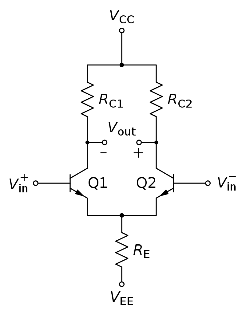
(a differential amplifier made with NPN transistors)
Then, there is the arrangement of transistor pairs Q13, Q14, and Q9, Q8, which form two current mirror circuits. Majorly, the purpose of the two-current mirror is to prevent a change in current flow in the internal circuit during voltage swings of an Op-Amp input. In addition, it reduces the chances of an override by maintaining the active operation range of the transistors.
Thirdly, the controlling transistors, Q12 and Q8, set the emitter-base voltage of the other transistor in the matching pair.
Also, to allow only a needed amount of current flow, you will maintain the voltage at the level fractions of millivolts. Later, the input circuit gets coupled with the first current mirrors Q9 and Q8 and then joins the output circuit with the second current mirror, Q13, and Q12.
Further on, transistors Q11 and Q10 form the third current mirror.
The two, having a high impedance connection, connect the negative of the power supply and the input circuit. It gives a reference voltage without giving loads to the input circuit. Also, it introduces a small base input bias current, a requirement of PNP transistors at the input of the common-base amplifier circuit.
Resistors 4.5 KΩ and 7.5 KΩ and the transistor Q15 prevent distortion of signals at the output amplifier stage by forming a voltage level shifter circuit. The shifter circuit works by dropping the voltage from the input amplifier circuit by 1V before proceeding to the subsequent circuit.
Again, you can use the transistors to Q20, Q17, and Q14 to form the 741 Op-Amp output stage. Then, transistors Q22, Q19, and Q15 will operate as class A amplifiers.
Lastly, transistors Q7, Q6, and Q5 equilibrate any loopholes occurring at the input differential circuit. Often, their arrangement enables them to take in two inputs, (an offset null positive and offset null negative) then proceed to balance the non-inverting and inverting inputs.
Note; The 741 Op-Amp design does not have a constant gain. Its variation is dependent on the frequency of the input signal. That is, as the frequency of the input signal increases, there is a reduction in the gain and the frequencies of about 100000 Hz.

4. 741 Op-amp Pinout
Op Amplifier 741– Pin2 and Pin3 (Input)
These are the input pins, with pin3 as the non-inverting input and pin2 as the inverting input for the integrated circuit. The two pins work simultaneously in that a greater voltage in pin2 than that of pin3 (higher voltage at the inverting input) lowers the output signal. On the other hand, a greater pin3 voltage than a pin2 (higher voltage at the non-inverting input) causes the output signal to go higher.
Op Amplifier 741– Pin4 and Pin7 (Power Supply)
The 741 IC draws power from these two pins, pin4 and pin7, to run its operation. Pin4 acts as the -ve terminal supply voltage, while pin7 is the +ve terminal supply voltage. In addition, the voltage at pin 4 and pin7 operate between 5V and 18V.
Op Amplifier 741– Pin6 (Output)
Pin 6 is the IC 741’s output pin. Its voltage is mainly dependent on the feedback mechanism in use and an input signal at input pins. At all times, a high output signal is an indication that the output voltage is similar to the positive supply voltage. Likewise, a low output would indicate an output voltage that is equal to a negative power supply.
Op Amplifier 741– Pin1 and Pin5 (Offset Null)
As it is in the specifications, a 741 op-amp provides a high gain rating. Thus, there can be irregularities during the manufacturing process or external disturbances occurring due to voltage differences in the inverting and non-inverting inputs. Consequently, it can disrupt the output.
And so, the purpose of pin1 and pin5 is to nullify the effect by applying an input offset voltage. To achieve the application, you will use a potentiometer.
Pin8 (N/C)
A pin 8 has zero connections to any circuitry in a 741 IC op-amp’s internal connection. Its role is majorly to be a dummy lead that fills empty spaces in a standard 8pin package.
5. Types of Op-Amps in use
The best way by which you can use the IC 741 Op Amp is to implement it in the open-loop configuration. The configuration is in both non-inverting and inverting inputs.
Inverting amplifier
As we had seen, pin6 and pin2 are the output and input pins, respectively. A voltage passed through pin2 gives output at pin6. A +ve polarity of the i/p pin2 leads to a -ve polarity at o/p pin6. Therefore, the i/p will always be opposite to the o/p.
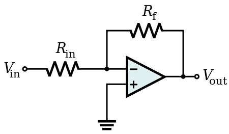
https://en.wikipedia.org/wiki/Operational_amplifier_applications#/media/File:Op-Amp_Inverting_Amplifier.svg (inverting amplifier configuration).
To calculate the inverting op-amp circuit, use the formula;
A = -Rf/R1
The negative sign is an indication of the polarity of the output waveform being in reverse.
Non-inverting amplifier
With this amplifier, pin6 is still the output pin whereas the input pin changes to pin3. A voltage given to pin3 will result in an output from pin6. A positive polarity at the pin3 input leads to another positive polarity on the o/p pin6. In this way, the o/p is not on the opposite side.
To calculate the non-inverting op-amp circuit, use the formula;
A = 1+ (Rf/R1)
Differential amplifier
As the name suggests, a differential amplifier amplifies the voltage difference present in non-inverting and inverting inputs.
For its calculation, use the formula;
Vout = R3R1 (V2-V1)

https://en.wikipedia.org/wiki/Differential_amplifier#/media/File:Op-amp_symbol.svg
(illustration of the formula)
6. Application of the Op Amplifier 741
A couple of IC 741 Op-Amp’s wide range applications include;
In generators
An op-amp 741 is applicable here as an oscillator in standard generators to generate varied output waveforms, e.g., the triangular, sinusoidal, square wave type waveforms, to mention a few. Additionally, you will find its application in Pulse Width Modulators/ PMW generators.
Creating DACs or ADCs
You can use a 741 op-amp to produce analog to digital circuits or vice versa. In cases of digital to analog converters, it’ll use digital binary input in the microcontrollers or computers to create a similar analog signal.
(microcontroller chips)
Op Amplifier 741–In rectifiers
Regular diodes usually have voltage drops making them inappropriate for high-accuracy signal rectifiers. The 741 Op-amp can act in place of a diode to eradicate the voltage drop.
Achieving computational tasks
Most electronic circuits performing mathematical tasks such as summation, differentiation, etc., make use of a 741 op-amp.
Other numerous devices that use an op amplifier 741 are;
A variable audio frequency oscillator.
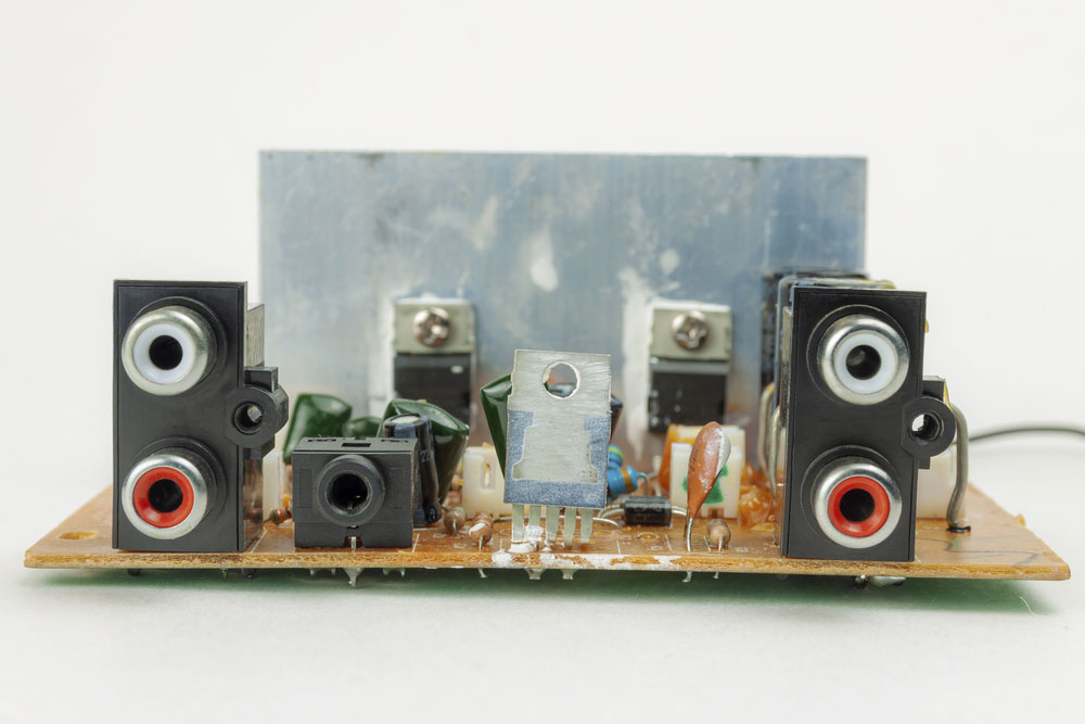
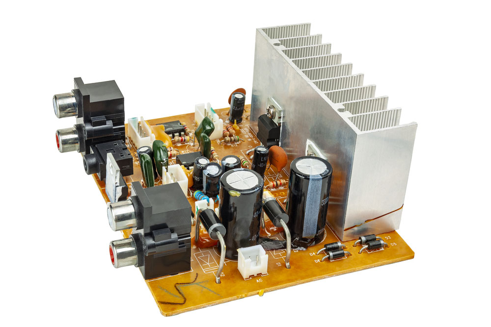
(an audio amplifier with IC Op-amp 741).
- DC volt polarity meter.
- Thermal touch switch.
- E-room thermometer.
- Audio mixture for four channels.
Conclusion
To conclude, we have managed to tackle the definition of an IC 741 Op Amp, its characteristics, product specifications, pinout, and applications. They make up the basics of an operational amplifier 741. For more details, inquiries, or more comprehension of the topic, contact us. We are at your service at all times.