Logic circuits may rely on a ripple carry adder to add n-bit values together. As a result, this digital circuit implementation provides useful features in many applications. However, it also exhibits delayed performance due to the slow calculation process. That typically involves waiting for each full adder stage to ripple the bits into the next full adder stage. Such a process repeats until it reaches the end, providing the results.
Understanding a ripple carry adder can seem a bit confusing. With that in mind, we put this article together to help you gain more knowledge on this subject. So let’s get started!
Contents
What is Ripple Carry Adder?
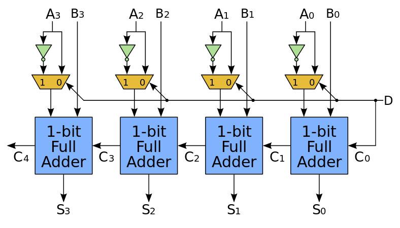
A ripple carry adder serves as a digital circuit that adds up two binary n-bit numbers and provides the results. Its structure consists of several full adders, with each one connecting in a cascaded setting. In this manner, the carry output of a full adder connects to the next full adder input.
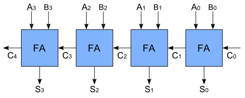
A diagram of a 4-bit ripple carries adder.
Source: Wikimedia Commons
A full adder represents a logic circuit designed to add three inputs while generating two outputs. More specifically, two inputs serve as A and B, while the third one depicts a carry-in bit. (C-IN) Meanwhile, one output represents a carry-out bit (C-OUT), and the other represents a sum bit (S). Ultimately, a full adder circuit can connect to eight inputs to form a byte-wide adder. This cascades a carry bit from one adder to the next. Joining two half-adder circuits together will form a full adder.
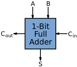
A complete adder logic diagram
Source: Wikimedia Commons
Ripple Carry Adder Working Principles
Each carry generates through a full adder stage, which will then proceed to the next full adder via its input. The whole process advances until it reaches the final full adder. As a result, each carry output bit ripples to the next full adder stage. Overall, the most crucial operation involves adding each input bit sequence together, such as 4-bit adder, 8-bit adder, 16-bit adder, etc.
Because of the logic circuitry’s propagation delays, the sum and carry-out bits remain invalid until the carry-in stage transpires. Propagation delays usually occur due to the amount of time passed between the input and the output. For example, when a NOT gate input sets to 0, the output will configure to 1, etc. Propagation delay defines how much time passed between the output setting to zero and input configuring to one. Also, the carry propagation delay defines how much time passed between receiving the carry-in signal and the carry-out signal implementation.
Ripple Carry Adder Truth Table
The truth table, as shown below, determines each output value for all the inputs in a ripple carry adders.
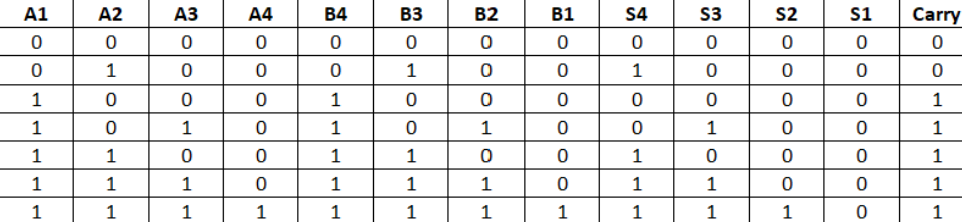
A ripple carries an adder truth table.
Ripple Carry Adder VHDL Code and Verilog Code
To implement a ripple carry adder, you will need the VHDL code and Verilog code. There are two examples provided. The first one involves a two-bit ripple carry adders. Meanwhile, the other example produces a ripple carry adder that collects each input width as a parameter.

Ripple Carry Adder Applications

Clocks contain a ripple carry adders
- Perform additions for two N-bit values
- Digital signal processing and microprocessors
- Timers
- Calculators
- Clocks
Advantages and Disadvantages of Ripple Carries Adder
Advantages
A ripple-carry adder is inexpensive.
Source: Wikimedia Commons
- Provides accurate results through n-bit addition
- Simple design and development process
- Inexpensive
Disadvantages

Delays cause an inconvenience for its overall functionality
- It only allows for one full adder to function at a time
- Carry bit delays cause it to run slowly
Carries Look Ahead Adder
A carry look-ahead logic calculates the carry-in bits before reaching the sum, effectively reducing the time delay. This occurs after generating the carry signal through two methods. The first one involves both a and b bits equating to one. Meanwhile, the second approach involves either the carry-in and a or b bits equating to one. These bits are implemented in the previous stage, while a carry-in starts at the beginning of the adder.
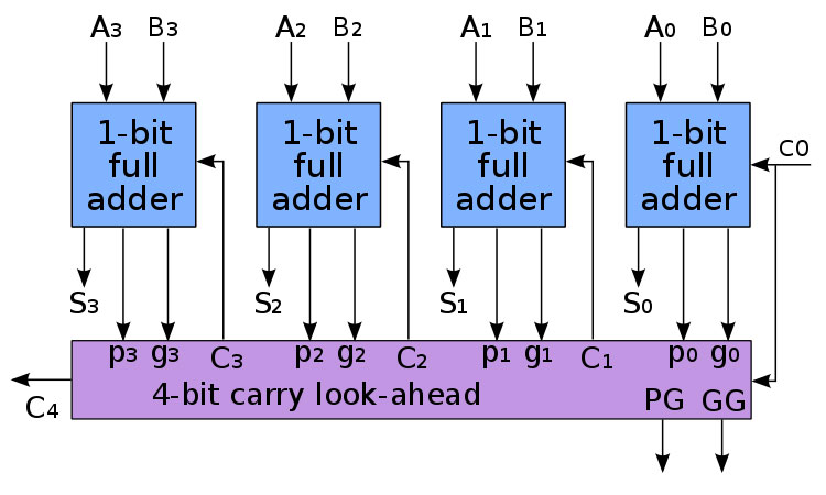
Carry look-ahead adder schematic.
Source: Wikimedia Commons
In a ripple carry adder, each full adder processes the carry-in bit to the next adder before calculating the sum. Therefore, that process results in a long delay.
Summary
Overall, a carry-ripple-adder provides the ability to add two n-bit numbers together in a digital circuit. Although a slow process, it still has useful applications that essentially help with digital signal processing. In this manner, a ripple carry adder ripples a carry-in bit to each full adder stage until it reaches the final full adder. At this point, it will then perform the needed calculations. However, carry-lookahead adders achieve this calculation quicker since it utilizes a different technique. Thus, reducing delay time.
Do you have any questions regarding a ripple carry adders? Feel free to contact us!