Contents
What Is A Flip Flop?
A flip-flop is a sequential logic circuit that has some form of built-in memory. Therefore, you can use the data from the current inputs, previous inputs, and (or) previous outputs to run through the system.
The circuit consists of several logic gates that result in two stable states (a logic level 0 or 1), making a flip flop a bistable multivibrator.
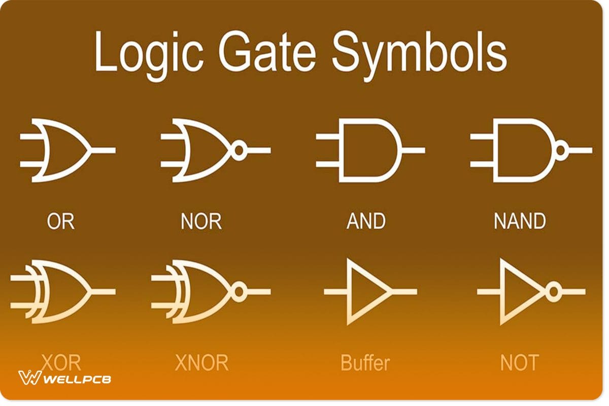
Different types of logic gates
The difference between latch and flip-flop circuits is that the latter are edge-triggered. Edge triggering means they have a control signal to coordinate the actions of the digital circuit. The control input is usually a dedicated clock signal, which makes them synchronous systems.
However, a latch circuit is level-triggered, which means its output can change if the inputs change. There is no clock pulse or clock event to activate them, so they are asynchronous systems.
It is worth noting that latches are the essential elements in flip-flop circuits, and they are volatile memory elements that lose their data if there is a power failure.
Types Of Flip Flops
There are four flip-flop types, each with a different circuit design and truth table.
SR Flip Flop
An SR flip flop gets its name from its S (set) and R (Reset) inputs.
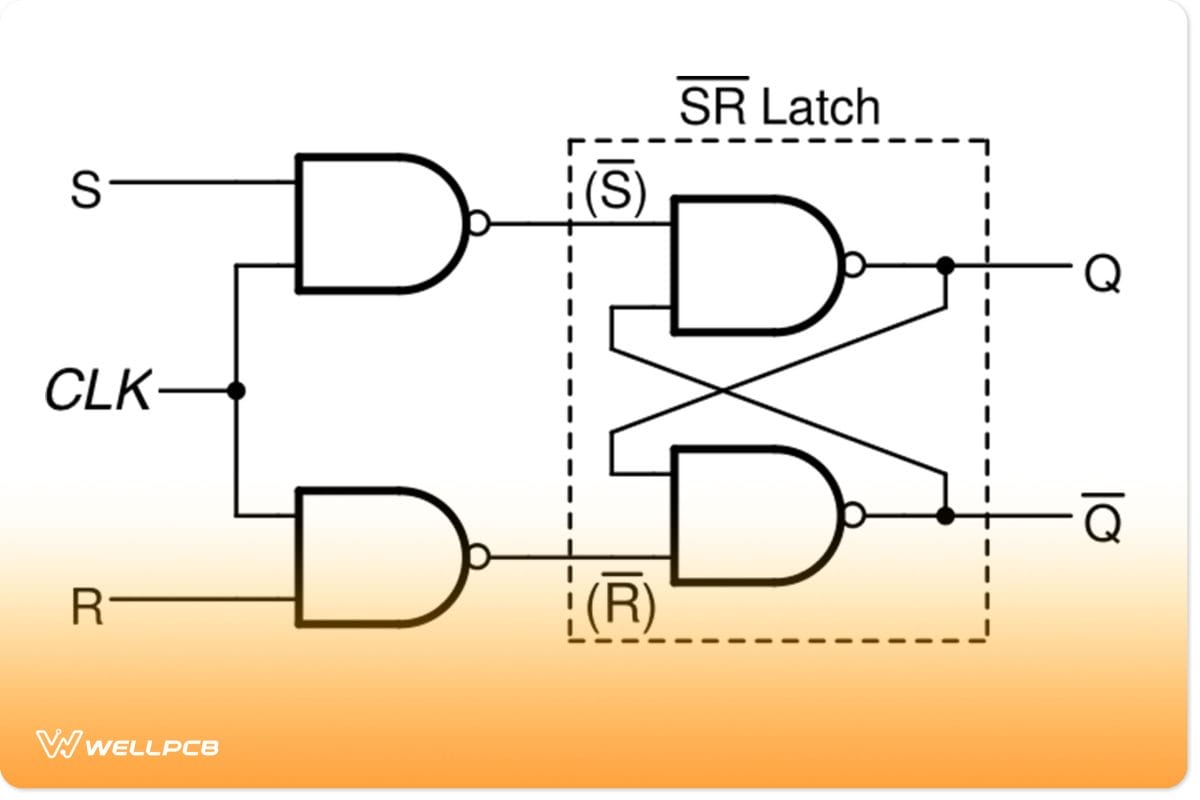
Clocked SR flip-flop circuit with cross-coupled NAND gates.
It is the most commonly used flip flop among the four, has the simplest circuit, and has a similar truth table to the SR latch.
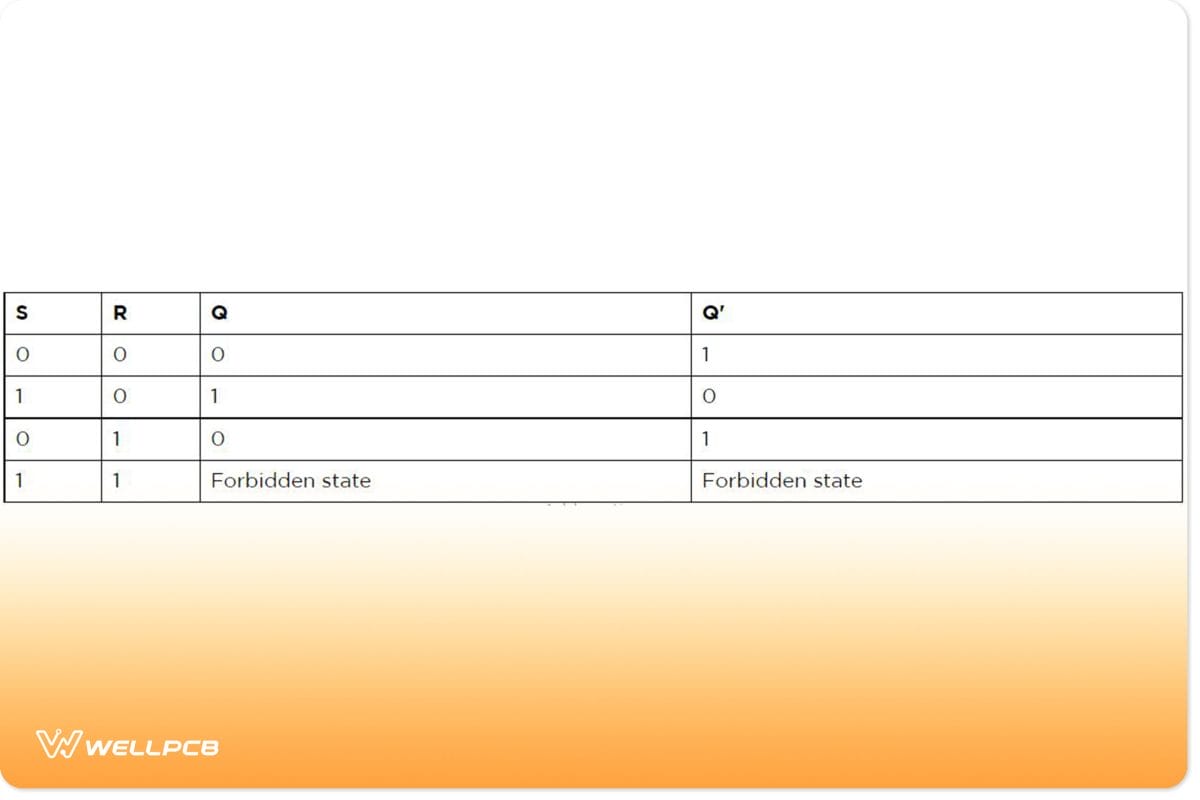
SR latch truth table.
JK Flip Flop
A JK digital circuit improves the design of the SR flip flop by ensuring S and R are not high simultaneously. By doing so, it eliminates the possibility of being in a forbidden state.
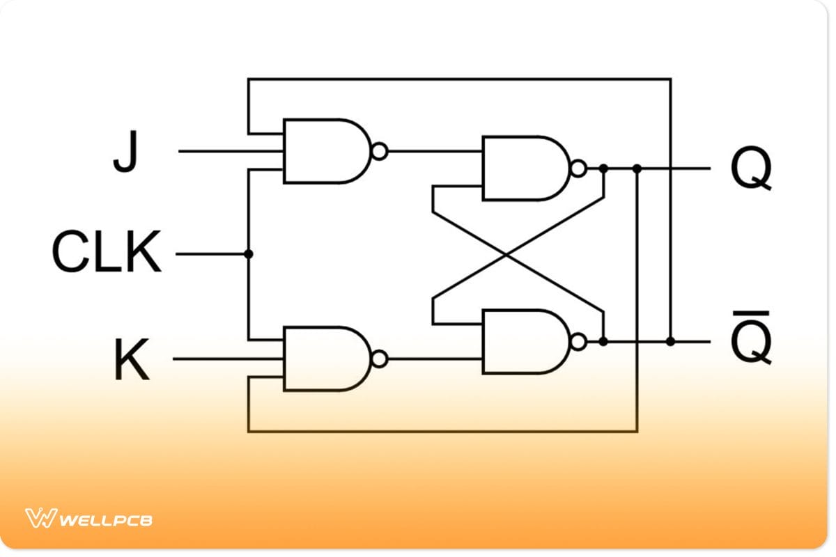
JK flip-flop circuit using NAND gates.
It has the following truth table.
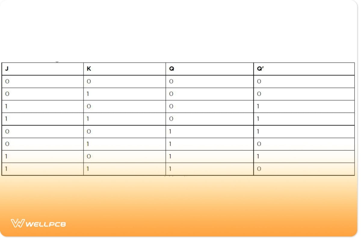
JK flip-flop truth table.
D Flip Flop
Also known as a “Data” or “Delay” flip flop, this circuit is a one-bit memory cell with one input pin (D). It is most commonly used in digital electronics systems to make registers and counters.
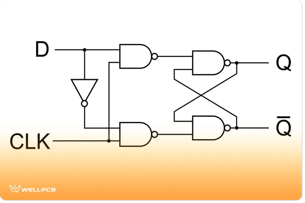
D flip-flop circuit using a NOT gate and 4 NAND gates.
The circuit’s output only changes at the clock’s rising edge, resulting in this truth table.
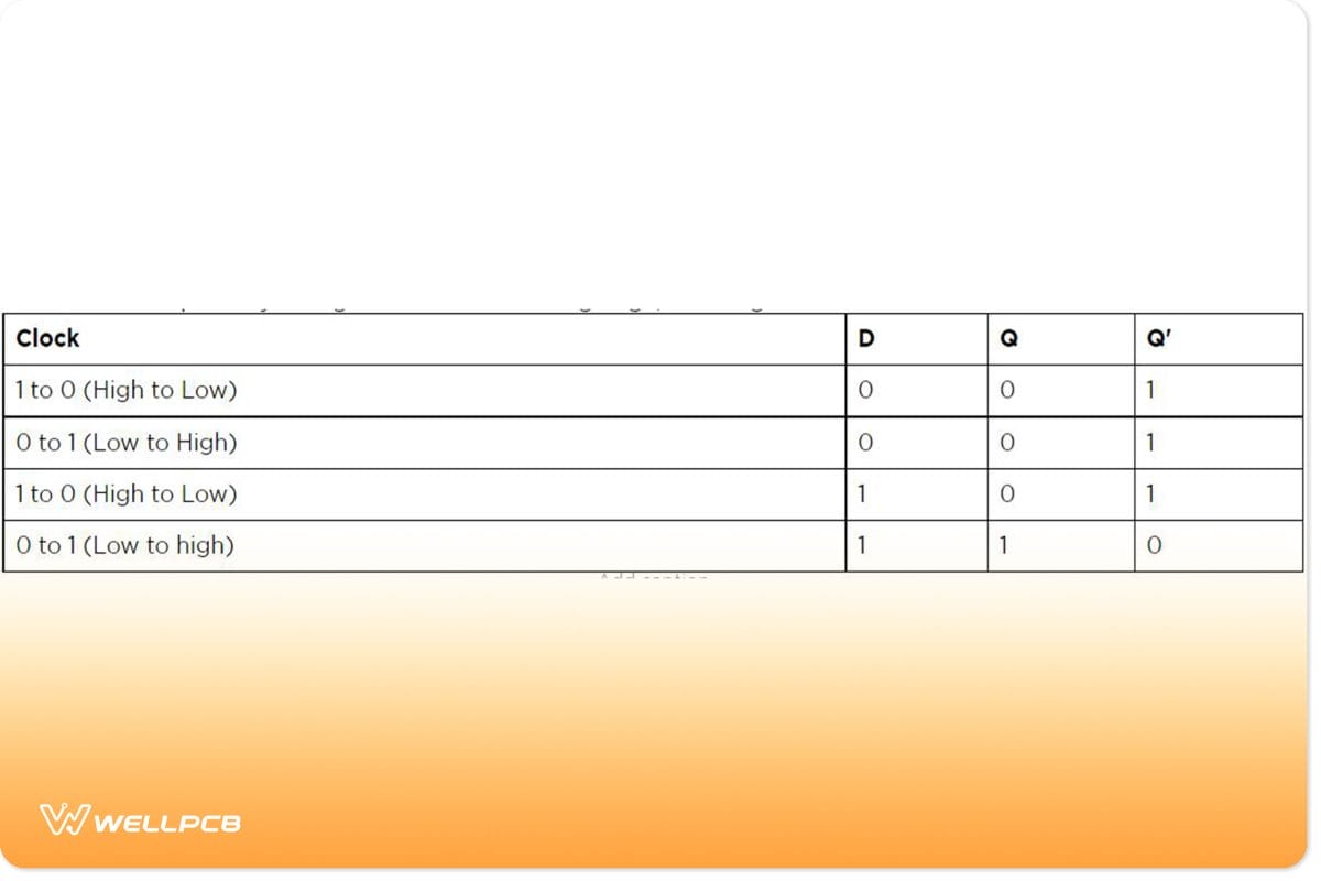
D flip-flop truth table.
T Flip Flop
A T flip flop is a single input version of a JK flip flop, connecting the two feeds to form a T input. The T stands for Toggle because the circuit can complement its state.
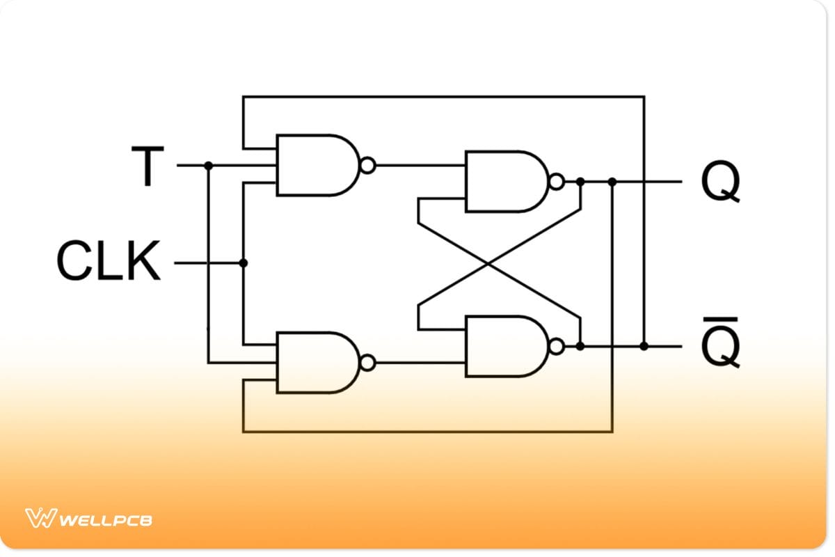
T flip flop circuit using NAND gates
The circuit presents this truth table.
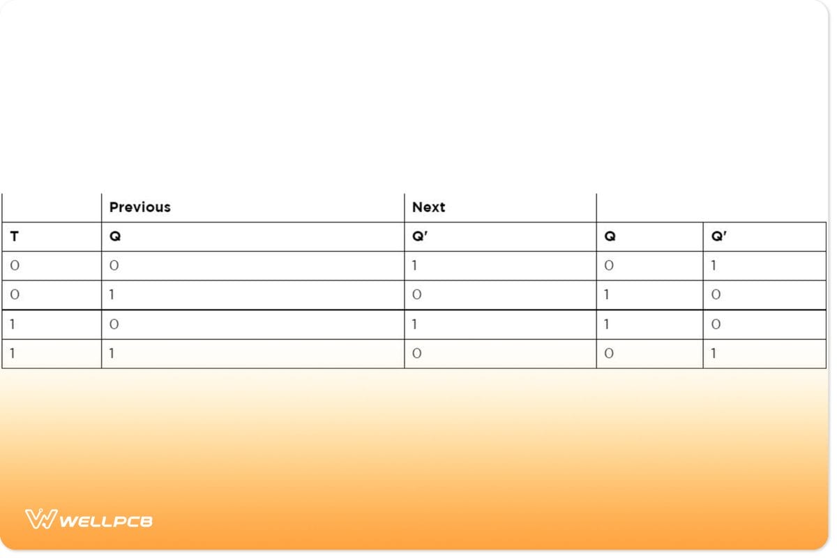
T flip-flop truth table.
Applications Of Flip Flops
- Counters
- Frequency dividers
- Storage registers
- Shift registers
- Latch
- Memory
- Bounce elimination switch
- Data storage
- Data transfer
- Registers
Transistor Flip Flop Circuits
Logic gates are the main elements in flip flops, but they are models representing logic in electronics. Real electric circuits have cross-coupled components to control this current flow. The values in their truth tables indicate either a binary digit 1 (high voltage) or 0 (low voltage).
They include components like transistors, resistors, and capacitors, and here’s how to make three of the most common circuits.
The One-Transistor Flip Flop
Like other conventional flip flops, the single-type transistor stores one bit of data; it has a set of set & reset inputs plus a feedback loop to keep the states stable.
Apart from the transistor (NPN), the circuit features a set of two diodes, two capacitors, six resistors, and an LED.
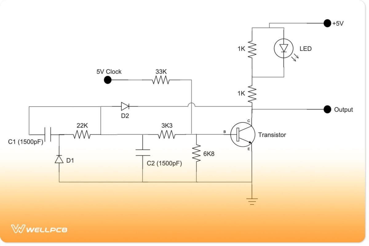
A one-transistor flip-flop circuit diagram.
From the diagram above, you can set the circuit by activating the supply voltage to C2. This 5V pulse raises the base voltage on the transistor and amplifies the clock signal. C1 and D1 will rectify the output signal, making the resulting DC voltage appear on C2.
The circuit maintains a positive feedback loop that keeps the flip flop in the ON state. D2 keeps the transistor from being saturated (having too much current), which prevents a continuous ON state that would eliminate the positive feedback signal.
To turn the circuit off, discharge C2 or remove the clock signal for a short period. Even if you connect the clock signal again, the flip flop will remain off because the 6K8 & 3K3 resistors and capacitor C2 heavily attenuate the high input.
D Flip Flop Circuit Using Transistors
A D-type flip-flop circuit has a gated D latch as the base of its wiring but adds on a clock circuit to make it an edge-triggered D flip-flop.
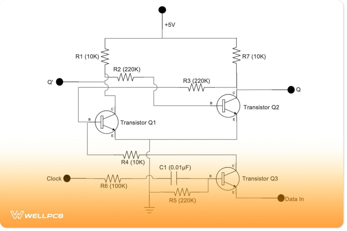
A D flip-flop transistor circuit diagram.
The lower section of the diagram consisting of the transistor, capacitor, and three resistors, forms the clock mechanism.
An external clock provides the base voltage, and the transistor can only transmit the input data when it has a positive base voltage.
The resistor R6 and capacitor C1 convert the square wave clock signal into sharp spike signals to identify the rising edge.
Overall, the latch section has two transistors and four resistors, and from this, the clock section, the current input heads to the latch transistor in the circuit.
If the output Q is a logic 0, you can apply a positive signal on the Clock pin and Data In pin. This action changes the stored data or state to one.
The clock input charges the transistor base and forward biases the base to the collector junction. Therefore, when the Data In positive signal comes in, it causes a small current to flow from the bottom to the collector and into the latch.
The current ends up triggering the latch, causing it to change its state to 1 at Q. To apply a logic 0, ground the Data In pin, and it will shift Q back to 0 and store this bit.
T Flip Flop Using Discrete Transistors
Toggle flip flops are very similar to Data flip flops, but instead of having a Data In input, the pin gets its signal from the complementary output Q’.
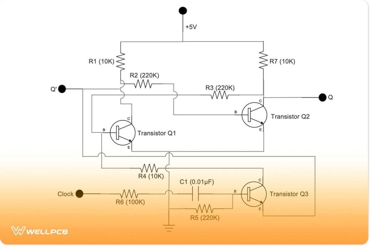
A T flip-flop transistor circuit diagram
The goal is to get a low data input when the output is high and a high data input when the work is low. Therefore, Q’ is vital in the equation.
However, since it is a discrete circuit, the system will not work because it is equivalent to connecting the transistor base to its collector. You can solve this problem by introducing an extra capacitor, C2, connected in series, and a resistor, R8, connected to the output Q.
The capacitor creates a lag between the input and output signals while the resistor discharges the capacitor. These two will ensure the transistor output is as expected, shifting states continuously.
Summary
In conclusion, transistor flip flops are the fundamental building blocks of most electronic and computer circuits due to their built-in memory function.
If your project requires such circuits, it is cheaper to buy the components described above and then build the unit yourself.
Get in touch with us to learn more about these components and the PCBs you need to set up the circuits.
