Varying transistor types exist on the market, many of which serve a unique purpose. Some also offer special features for specific circuit applications. In this article, we discuss the Transistors MESFET, a field-effect transistor. This semiconductor device can control current flow through the channel, making it ideal for RF implementations. Other characteristics also ensure that it achieves high performance. Professionals will need to understand the MESFET and its working conditions before integrating it into circuits. This article will help you take a close look at the device. So let’s get started!
Contents
Metal-semiconductor Dield-effect Transistor
A MESFET (metal-semiconductor Field Effect Transistor) is identical to a JFET’s operation and construction, but with one main difference. Generally, it features a Schottky junction rather than a p-n junction to alter the depletion region’s width and control conduction. With this in mind, you can implement a MESFET in high-power RF circuits applications.
On the other hand, you can also utilize a GaAs (Gallium arsenide) MESFET, which has improved electron mobility for high frequencies. It features an active layer and a semi-insulating substrate with low parasitic capacitance. The GaAs MESFET provides excellent performance for applications requiring high power (40W) and low power. For example, this includes radar, satellite communications, and microwave communication.
Types of MESFET
Two MESFET types exist on the market today, N-channel and P-channel. However, the N-channel is more popular due to its electrons acting charge carriers. This type also provides 20 times more electron mobility than GaAs hole mobility.
MESFET Construction and Working
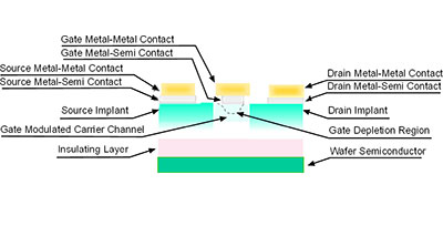
A MESFET contains a single ultrathin, lightly n-doped semiconductor layer referred to as a channel. The channel engraves on a semi-insulating substrate having heavily-doped semiconductors on both ends, known as the source or drain. Meanwhile, metal covers the channel’s top portion, which forms the Schottky junction, fabricated between the two terminals. This area also represents the gate terminal.
When the gate sets to a negatively biased condition, it controls the channel’s current flow. To achieve that, it will generate a charge carrier-devoid depletion region close to the metal-coated gate. In effect, this process, called carrier channel width modulation, restricts channel current.
MESFET Symbol

Image representing the MESFET symbol.
The depletion region widens in the gate terminal. In the symbol, as shown above, the P-channel’s arrow points outward while the N-channel’s arrow points inward.
MESFET Operation
Overall, the MESFET operates in two modes, enhancement and depletion mode:
Enhancement mode MESFET: In this mode, the depletion region has sufficient space to block off charge carriers from gate to source. Additionally, the MESFET sets to an off state by default. It also receives positive voltage between the gate and source terminals, shrinking the depletion region. As a result, the channel generates a current. However, a large current flows when the Schottky diode’s junction sets to forward bias due to the positive gate-to-source voltage.
Depletion mode MESFET: The MESFET operates in depletion mode when the depletion region fails to expand to the p-type substrate. Generally, this mode will activate without a negative gate-source voltage. After applying a negative voltage, the MESFET depletion-mode will deactivate, increasing the depletion region’s width. Thus, it prevents the flow of charged carriers from the source to the drain.

MESFET Characteristics

A MESFET provides high electron mobility.
The main MESFET characteristics include:
High input impedance: MESFETs offer higher input impedance than bipolar transistors because of the diode junction.
Oxide trap prevention: Unlike the popular silicon MOSFET, a MESFET can prevent oxide traps.
High geometry control level: Additionally, MESFET provides improved channel length control compared to the JFET. A high geometry control enhances the product’s performance, allowing small geometries for RF radio frequencies.
Low capacitance: Overall, a Schottky diode gate structure provides low capacitance levels, ideal for RF and microwave applications.
Negative temperature coefficient: The MESFET can prevent thermal issues from occurring due to its negative temperature coefficient.
High electron mobility: Amplifiers with MESFET semiconductor technology, which provides high electron mobility, operate at frequencies between 50GHz and 100GHz.
Applications of MESFET

Cell phones commonly feature a MESFET.
MESFETs integrate into many applications, including:
- Cell phones
- Microwave circuits
- Satellite communications
- RF amplifiers
- Radar
- High-frequency devices
- Commercial optoelectronics
- MESFET advantages and disadvantages
A MESFET Offers Some Distinct Advantages Along with one Main Disadvantage:
Advantages:
- High-frequency operation
- Designed without an oxide layer to prevent oxide traps
- High geometry control level
- High input impedance
Disadvantages:
- The GaAs Schottky diode’s turn-ON voltage sets to 0.7V. As a result, the threshold voltage must be less than this value. As a result, this feature will make it difficult to produce circuits requiring enhancement-mode MESFETs.
MESFET vs. MOSFET
The main difference between a MESFET and MOSFET involves their operational capabilities. In this case, a MOSFET sets to the off state until its gate receives voltage higher than the threshold. Meanwhile, the MESFET stays on by default until it gets a reverse voltage.
Summary
Overall, a MESFET features a gate, source, and drain terminal, similar to a JFET. Plus, the gate terminal serves as the Schottky junction, which consists of a metal coating. This region controls the depletion zone width when the device activates or deactivates. Such a configuration also makes the transistor different from JFETs, which rely on a p-n junction. Moreover, you can integrate a GaAs MESFET on circuits requiring higher frequencies.
Do you have any questions regarding the MESFET? Feel free to contact us!