The 74HC00 IC belongs to a logic family of the 7400. This IC is a 14-pin quad 2-input NAND gate with four independent gates. Also, each gate is capable of performing a NAND function. The NAND gates use advanced silicon-gate CMOS technology to achieve high operating speeds. The operating rates are similar to the LS-TTL gates with the low power usage of a standard CMOS integrated circuit.
This article discusses the 74HC00 IC, where to use it, and how to use it.
Contents
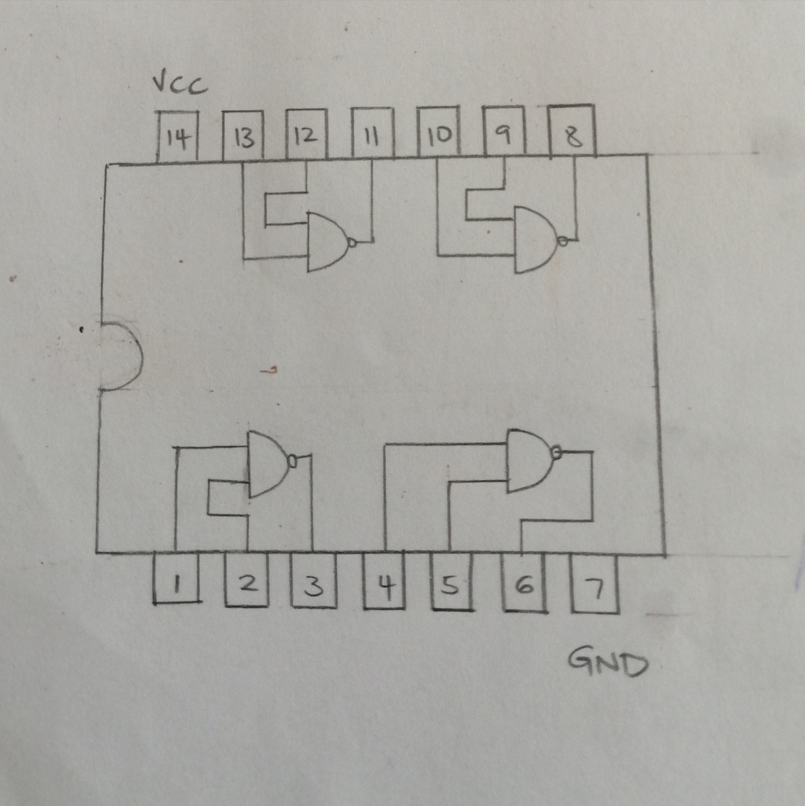
74HC00 Pinout Configuration.
The 74HCC00 device has a 14 pin arrangement. Notably, these pins are both the input pins and the output pins. The statements below describe each pin on the device.
Pin 1,4,11, 14 are pins(A) NAND gate inputs and serve as the first input pins for the gate.
However, pin 2,5,12,15 are also NAND gate inputs classified as pins(B). Contrary to pins(A), pins(B) are the second input pins.
Pin 3,4,12,13, classified as pins(Q), are the NAND output pins. These pins serve as the output pins for a different gate: the OR gate.
Pin 7 is simply the ground pin, and it earths the circuit.
Pin 16 is the VCC, also referred to as the VDD, and it supplies a +5v power to the IC.
(an integrated circuit showing its pins.)
What is 74HC00 IC?
The 74HC00 is a standard Quad 2-input TTL NAND gate integrated circuit. This IC belongs to a series of 7400 digital logic gate systems. These ICs get the name because you can solve any logic functions using the NAND gates. Also, NAND means a negated version of, AND hence a NAND output complements the AND output. For example, if FALSE is the NAND output, then this means that all the inputs are TRUE and vice versa.
Features or Technical specifications
- Firstly, the operating voltage range is between -0.5v to7v.
- Secondly, the IC is a quad 2-input NAND gate.
- Thirdly, this TTL device has a typical operating voltage of 5v.
- Also, the maximum propagation delay with a 5v supply is at 28ns.
- Further, 74HC00 has a DC input current of ≶20mA.
- This IC has a 3.15v minimum logic high voltage with a 5v supply.
- Also, 1.35v is the minimum logic low voltage with a 5v supply.
- Lastly, these logic gate systems come in a 14-pin PDSO, PDIP, and GDIP package type.
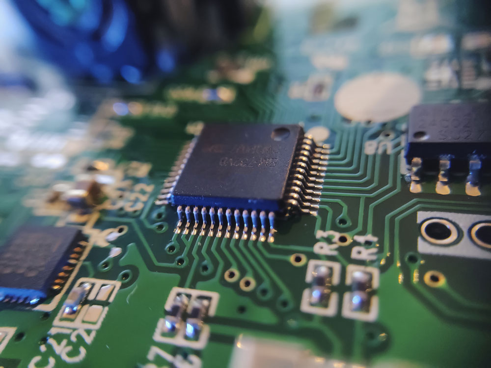
(an IC on a circuit board.)
Replacements and equivalents.
Like any other electrical equipment, the 74HC00 IC has equivalents, namely the CD4011 and the SN54LS00. Also, you can reconfigure any two transistors into a double, which will create a NAND gate.

Where 74HC00 IC is used
We have some situations where the 74HC00 IC is necessary for electronic circuits. The primary function of this IC is performing NAND functions. Also, each NAND gate of the 74HC00 IC has a specific role.
If you want a logic inverter, the NAND gates present will change to NOT gates. Consequently, it is possible to make NOT gates from NAND gates when the situation arises.
Also, when you need a quick NAND gate operation, the 74HC00 chip is perfect for the job. Importantly, this IC has fewer transition times required for faster applications. Therefore, you can use the chip in systems that require higher frequencies.
The 74HC00 IC is popular since it is very affordable and available in local markets.
(an electronic circuit with ICs)
74hc00 Pinout:How to use 74HC00 IC?
As aforementioned, this IC has four strategically placed NAND gates.
(the interior connections of the NAND gates.)
Note: NAND gate is a combination of the AND and NOT gates.
However, like all gates, the NAND gate has a truth table.
| input 1 | input 2 | AND output | NAND output |
| 0 | 0 | 0 | 1 |
| 1 | 0 | 0 | 1 |
| 0 | 1 | 0 | 1 |
| 1 | 1 | 1 | 0 |
0= low input 1= high input
74hc00 Pinout:Circuit Example
Look at the circuit below to further understand how the NAND gates operate.
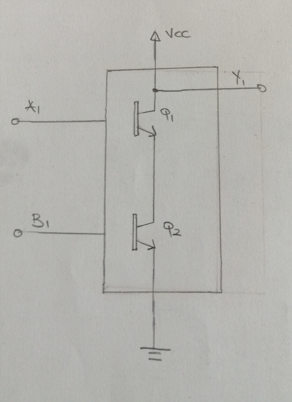
(an internal circuitry of a NAND gate.)
From the circuit, whenever points A1 and B1 are 0, this turns OFF transistors Q1 and transistor Q2. Therefore, the total supply voltage is shown on the Q1 and Q2 transistors. Since output Y1 is the voltage across the transistors, Y1 will record value 1.
However, just the corresponding transistor will work in a scenario where a single input is high. Therefore, the other goes OFF. You will record the entire supply voltage on the OFF transistor in such a situation. Since output Y1 is the voltage across the transistors, Y1 will be high.
But when all device inputs are 1, this turns ON both transistors. However, the supply voltage covering the two transistors will be a blank output.
Therefore, the entire output Y1 will be 0.
The statements above help to justify the truth table given above.
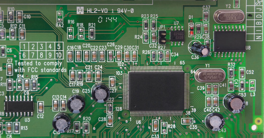
(ICs and other electrical components fitted on a PCB.)
74hc00 Pinout:Application Circuit
You can see a simple application circuit for a NAND gate below.
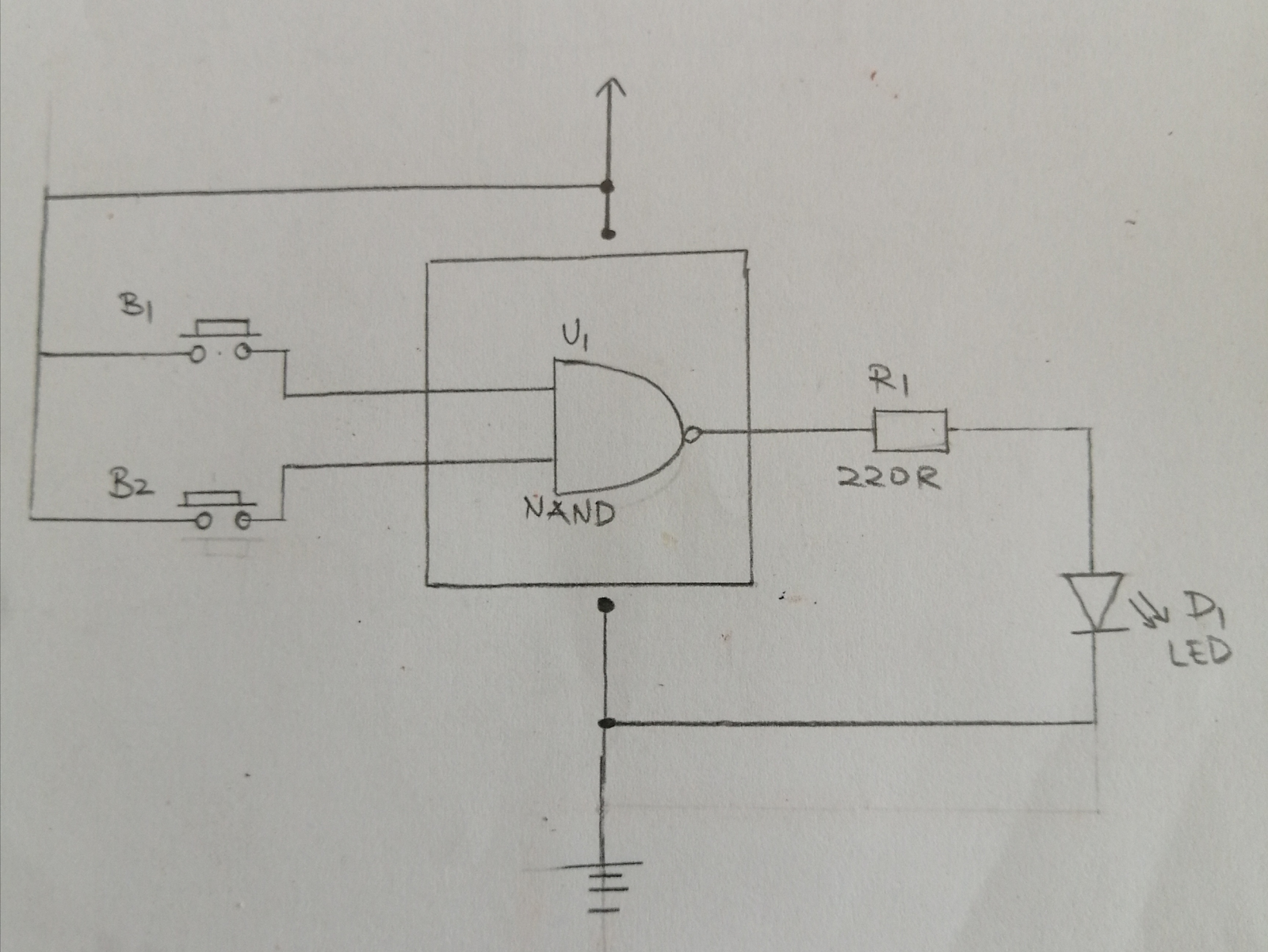
(application circuit for a NAND gate.)
In this circuit, we combine the two input buttons, and the output connects to the LED. When this LED goes ON and OFF, you can then identify the work of the logic gate of the system.
When in the default setting, the two input buttons are usually open. Consequently, low input at the gate occurs. However, when the two inputs are 0, the output will be 1, resulting in the LED turning ON.
Contrastingly, when you close both buttons, one of the inputs will be 0. Whereas the other will be 1. In such a case, the collector output will be 1, turning ON the LED.
If you press both the buttons, the result will be low output. This low output will turn OFF the LED.
The three cases discussed to explain the table above and how to use the NAND gates to achieve your results.
(an electronic integrated circuit chip.)
74hc00 Pinout:Applications
- Firstly, you can use the logic quad 2-input NAND gates in digital circuits.
- Secondly, this IC’s output voltage range allows for oscillator circuit application.
- Thirdly, 74HC00 has a low power consumption therefore suitable during encoding and decoding.
- Also, you can use the IC when multiplexing and de-multiplexing.
- Additionally, you can apply the 74HC00 IC in a basic logic circuit.
- Lastly, you can use these logic quad 2-input NAND gates in networking and programmed systems.
(a photo of ICs)
Summary
We hope this article answers any of your questions. Also, do not hesitate to contact us for additional information.