Contents
- 1 What is a BGA?
- 2 What is an LGA?
- 3 What is a CPU Socket?
- 4 Installing CPU on Land Grid Array Socket Motherboard
- 5 LGA vs. BGA
- 6 BGA vs. LGA: Which is Better?
- 7 How to Solder the LGA Package?
- 8 Common LGA Soldering Problems and Solutions
- 9 LGA Inspection: What Techniques Are Available?
- 10 What does FCLGA Mean?
- 11 What is the LGA Packaging Process?
- 12 Applications of LGA and BGA Components
- 13 Factors You Should Consider When Picking Between LGA and BGASeveral factors must be considered.
- 14 FAQs:
- 15 Last Words
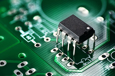
What is a BGA?
The Ball Grid Array (BGA) is an IC package that precedes the Pin Grid Array (PGA). While the PGA uses pins to connect to a PCB, the BGA uses pads with tiny solder balls.
BGAs can only work with PCBs with copper pad patterns matching the solder balls. You can place the solder balls manually or automatically. Tacky flux helps BGAs stay in place during assembly.
After the assembly, manufacturers heat the BGAs with an infrared heater or in a reflow oven.
This process melts the solder and secures the package to the PCB.
Also, the BGA will have correct alignment and proper separation distance –from other components.
Once the solder cools and solidifies, it will connect the BGA to the PCB.
Sometimes, solder balls are found on the package and PCB. They connect two packages.
What is an LGA?
The Land Grid Array (LGA) is an IC package with pins on the socket instead of the IC. However, this only applies when a PCB has a socket connector.
If your PCB doesn’t have a socket, selling LGAs to the board is possible.
LGAs have rectangular contact grids (“land”) on their undersides. Also, you don’t have to use all the grid rows and columns.
Additionally, manufacturers can make these lands with solder paste or LGA sockets.
Also, the grid elements can have different polygonal shapes and sizes, like triangular or circular. Some may even have a honeycomb appearance.
Manufacturers usually optimize their designs for factors such as getting the best shape for matching spring contacts, contact likeness and proper electrical distance to nearby contacts.
What is a CPU Socket?
CPU sockets on PCBs utilize different pins that help connect a CPU to a computer motherboard.
In addition, CPUs connected via sockets don’t need solder, allowing easy replacements.
Additionally, manufacturers often use CPU sockets for desktop gaming PCs, while laptops mostly have soldered versions.
Choosing a motherboard goes beyond getting the features you want.
So, it would be best to examine whether the motherboard has a CPU socket supporting your CPU model.
So, it doesn’t matter if you have a state-of-the-art CPU.
However, it won’t work if you have the wrong socket. Manufacturers like Intel and AMD have different CPU socket types for their mainstream and high-end desktop CPUs.
Installing CPU on Land Grid Array Socket Motherboard
The first thing to know is that the motherboard’s pins slot into the CPU instead of the CPU’s pins slotting into the motherboard.
This makes installing the microprocessor/CPU a lot easier.
When installing the CPU, you’ll first notice that the motherboard has a bracket that locks the CPU.
You can unlock the bracket by pulling its lever. Once that’s done, you must align the CPU chip with the bracket as accurately as possible so that the CPU connects correctly.
Most LGA motherboard brackets have a margin of error of 2mm.
Once you’ve ensured that you’ve correctly slotted the CPU in place, use the lever to lock the bracket into place.
LGA vs. BGA
Now, let’s examine closely how these grid arrays differ and what they can be used for in a PC circuit.
LGA vs BGA: Pros and Cons
Pros of BGA
- BGAs don’t take up a lot of space because of their small sizes. In other words, they allow for optimal space utilization. But irrespective of the size of these IC packages, it’s possible to create small and powerful gadgets.
- It’s easy to unsolder BGA packages. And the process doesn’t damage the PCB or IC package.
- You can remove old and worn-out solder balls from your BGA package through deballing.
- Also, you can add new solder balls to your package through the rebelling process.
- It’s rare for BGA packages to overheat because they have excellent heat dissipation capabilities.
- BGA chips are not permanent. Therefore, they are easy to unsolder. And you can move them to other devices without any damage. Also, you can use the deballing and reballing process if the solder balls are weak.
- You can use the BGA as a computer CPU because of its excellent thermal and mechanical properties.
- BGAs boast short lead connection paths, which results in low-impedance features and the ability to generate signals quickly.
Drawbacks of BGAs
- It’s not easy to inspect solder joints on a BGA package. You’d also need X-rays to access the component-to-PCB connection since BGAs use their bellies to make connections.
- You can’t use BGA packages for many applications because they can only operate on multi-layered circuit boards.
- Although it’s easy to unsolder, you’d need special equipment to solder these packages to the PCB.
- Carrying out BGA repair can be a bit tricky, and you’ll need expertise and special equipment to execute it.
Pros of LGAs
- Due to their small size, LGAs are space-efficient, and you can use them to build small, powerful devices.
- LGA packages are more durable and won’t get damaged easily. Why? Because the pins are on the board, not the CPU. Also, the socket’s bear points have impressive durability.
- LGA pins are tiny, allowing manufacturers to fit many pins in a small area.
Cons of LGAs
- Although LGAs aren’t damaged easily, they can be expensive to fix if problems occur.
LGA VS BGA: Components
LGAs don’t use balls for connections. Instead, they use flat contacts that need sockets or direct soldering to connect to a PCB.
In contrast, BGAs use balls to connect to PCBs. Manufacturers usually attach these balls to the bellies of these packages.
LGAs vs. BGAs: Ease of Connection and Replacement
LGAs are pretty easy to connect to a PCB. Usually, these PCBs come with sockets to insert your LGA CPUs. Also, there’s no unique replacement process–you only need to remove the old CPU and insert the new one.
On the other hand, BGAs need special equipment to connect and remove them from their CPU sockets. Though it’s almost risk-free, the process is still more expensive than LGA packages.
LGA vs. BGA: Use in Microprocessors
Top manufacturers like AMD and Intel prefer using LGA packages over BGA, especially desktop gaming PCs.
Moreover, some manufacturers still use BGA to mount microprocessors, WiFi chips, and FPGAs permanently.
BGA vs. LGA: Which is Better?
BGAs and LGAs are great. But your choice should depend on preferences or what is best suited for your project requirements.
The biggest difference between Land Grid Array (LGA) and Pin Grid Array(PGA) packaging is the pin configuration.
LGA integrated circuits use flat pads, whereas the PGA counterpart sports protruding pins.
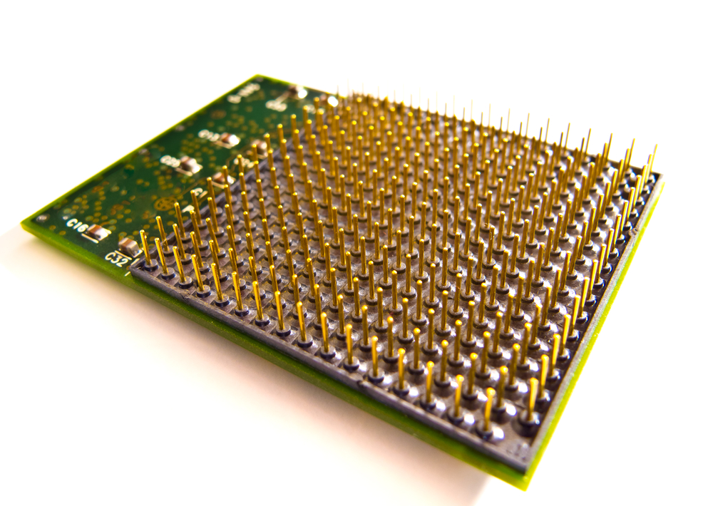
Back Side PGA CPU Card With Gold Pins
Because of their designs, LGA chips tend to last longer than PGA chips. However, PGA motherboards tend to last longer than LGA variants.
Installing CPUs on PGA motherboard sockets is easier, but the CPU pins tend to be very sensitive and easy to bend.
However, LGA sockets deliver a more reliable power supply. Moreover, they’re far more durable.
Intel typically uses the LGA sockets and packages for their processors, whereas AMD uses PGA. Ultimately, which you choose depends on your preference. However, LGA microprocessors tend to be more affordable.
How to Solder the LGA Package?
The first step to soldering an LGA package is preparing the PCB.
You need to ensure that it’s free from contaminants and oxides and that the wetting process is as effective as possible.
The best way to do this is to apply flux to the pads.
Once that’s done, you proceed with the soldering process, which you must follow with inspection. Inspection of the soldered LGA package involves visually analyzing the integrity of the joints.
Using x-rays is one of the most reliable inspection techniques.
Once you’ve ensured that there are no defects, you can move on to the next step – cleaning.
You need to remove any residue left by the flux and other contaminants.
Any leftover residue may corrode the PCB if you fail to do this. Once that’s done, allow the solder to cool and harden at room temperature.
Inspect the PCB once again, ascertaining that there is no damage, defects, or anomalies.
If you find any imperfections, you’ll need to re-work or repair them.
Once you’ve soldered the LGA package, power the PCB on to see if all the connections function as intended, and then clean the PCB again with isopropyl alcohol.

Common LGA Soldering Problems and Solutions
LGA packages suffer from the same soldering issues affecting other soldered electronic components.
These include bridging, tomb-stoning, non-wet opens (NWOs), Head-on Pillows (HOP), and pitting. Some of these issues result from insufficient solder.
As such, it’s important to ensure there is enough solder during the wetting and soldering process to prevent some of these problems from occurring.
You canalso prevent other issue,s such as tomb-stonin,g by increasingthe oven temperature and ensuring thatthe soldert distributes evenly.
LGA Inspection: What Techniques Are Available?
We previously mentioned two LGA inspection methods – manual visual inspection and X-ray inspection.
In addition to these two techniques, you can also use optical inspection, electrical testing, and environmental testing.
The best results are obtained by using a combination of tests and inspections rather than a single technique.
What does FCLGA Mean?
A flip-chip land grid array package (FCLGA, which adds a controlled collapse chip connection to the package.
In this configuration, the chip is inverted and connects to its substrate through small protrusions (bumps) or balls.
What is the LGA Packaging Process?
The LGA packaging process is very similar to the soldering process. It involves die preparation, solder deposition, reflow soldering and PCB cleaning.
First, the manufacturer cuts a chip from a larger wafer and then places it in protective material.
The manufacturer then covers one face of the chip with a series of miniature solder balls.
Next, the manufacturer heats the chip to melt the solder balls.
This process forms connections in the chip. The manufacturer then cleans the package.
Applications of LGA and BGA Components
Land Grid Array (LGA) and Ball Grid Arrays(BGA) packages have use cases in computing technology.
However, they do differ slightly in which components they’re implemented in.
You can find LGA technology in Intel processors, ethernet controllers, and power MOSFETs.
Similarly, BGA packages can be found in graphics processing units (GPUs), System-on-chip (SoC) processors, field-programmable gate arrays (FPGAs), and memory controllers.
Factors You Should Consider When Picking Between LGA and BGASeveral factors must be considered.
There are several factors you must consider when choosing between LGA and BGA packages.
These include pin count, repairability, thermal performance, size, signal integrity, cost, and mechanical stability.
FAQs:
What is the easiest IC package to manually inspect?
Many experts consider the Quad Flat No-lead (QFN) package the easiest to inspect without using tools such as X-rays and magnification. This is primarily because of the QFN package’s exposed pads, which provide clear visual access to the solder joints.
Which IC packaging has the highest pin count capacity?
Generally, BGA packages tend to have the highest pin count capacity. They can accommodate a pin count as high as 1500, while LGAs tend to have a limit of 500 pins.
What package offers the most design flexibility?
LGA packages offer the most design flexibility as they utilize interconnect sockets.
This lets you easily upgrade or replace components without breaking the solder connections.
We cannot say the same for BGA packages, as once you solder them, they are permanent.
Which package is best for thermal management?
The LGA package is the best for thermal management.
This is because of its exposed metal landframe. It facilitates exceptional conductive cooling.
Last Words
LGA and BGA are excellent IC packages that have been around for many years.
And, despite their drawbacks, the performance of these IC packages has led to many tech advancements.
For instance, these packages have produced powerful gadgets and devices like phones, smartwatches, tablets, etc.
Also, they allow you to use PCs with powerful performance.
What do you think about the LGA and BGA packages?
Do you need help with how to use these packages effectively?
Please feel free to reach us with questions.