Contents
- 1 1. What is IC packaging?
- 2 2. What are the types of IC packaging?
- 3 3. Through-hole Mounting VS Surface Mounting
- 4 4. Integrated Circuit Packaging Material
- 5 5. Assembly method of IC packaging
- 6 6. How Should We Choose the Type of IC Packaging?
- 7 7. Uses and advantages of IC packaging
- 8 Why Is IC Packaging Important?
- 9 IC Packaging Design Considerations
- 10 Summary
1. What is IC packaging?
IC is the material containing a semiconductor device. You can see them if you open your printed circuit board.
On the other hand, the package is a case surrounding the circuit material to protect them, especially from corrosion.
It also gives room for easy mounting of electronic contacts on a PCB.
Inmanufacturingf ICs, the packaging is essential, though it comes last in the process.
Therefore, IC packaging is the encasement whose aim is to shield electrical components from physical damage and corrosion.
It also assists in holding leads and contact pins that connect a device from external circuits.
2. What are the types of IC packaging?
Two types of IC packaging are mostly standard. They depend on their manner of mounting on a printed circuit board. They are:
2.1 Through-hole mounting package
The design of the through-hole mounting package is simple. Here, you mount the lead pins through a single side of the board and solder on the other part.
They find heavy useofn electronic equipment to compensate for a board’s cost limitations and space.
Under through-hole mounting, wne find the following types of packages:
DIP package :
These are some of the most heavily relied upon IC packages. If you’re keen enough, you’ll notice that the pins are parallel.
They also extended somewhat perpendicularly and were laid out on some black plastic housing, which is rectangular in most cases.
The package sizes will vary based on the size and the difference in the PIN. Mostly, the numbers range from 4 to 64.
There are several types of DIP Packages. However, the most common are Molded Dual In-Line Packages (MDIP) and Plastic Dual In-Line Packages (PDIP).
Standard :
Standard is another type of through-hole mounting package. If you didn’t know, Standard is the most common and popular type of IC packaging.
Many PCB assemblers and those in the electronics industry rely on this type of packaging. The pins here are 0.1 inches apart.
The space between the terminal rows in this type of packaging is 7.62mm.
Shrink :
Shrink is also another popular through-hole integrated circuit mounting package. Even though shrinks are quite similar to standard ones, the lead pitch is 1.778 mm. They are a bit smaller and tend to employ high pin-density packaging.
Zigzag (ZIP) in linear package :
Pins are inserted perpendicular to the circuit board in this type of packaging. The pins in the package are aligned vertically and tend to sit close to each other.
Zigzag linear packaging wasn’t that popular across the electronics industry. Zigzag goes down in history as a short-lived technology that mostly saw its heavy use in dynamic RAM chips.
Today, not many electronics makers use it anymore as IC packages. Most of them rely on DIP PackagAlthough and Shrink Packaging.
2.1.1 Surface mount packaging
Surface mount packaging is the technology that involves picking and placing components on a bare PCB.
While this fabrication process is quite fast, it may come with defects on the other side. Defects may arise due to the miniaturization of components, which is common in this type of technology.
When parts are placed close to each other, defects are impossible to detect. Nevertheless, this is a form of IC packaging.
Manufacturers can achieve surface-mount IC packaging in two ways, as explained below:
Small size L-shaped lead package -This type of packaging consists of gull-wing type leads.
These leads tend to draw out correctly in either direction in an L fashion from the body.
Manufacturers can easily mount them on the board using their simple rectangular shapes with horizontal edges.
These packages are prevalent in integrated circuits that power flash memories and RAM.
Ball grid array (BGA) -A ball grid array or BGA, in short, is a chip that carries a surface-mount package mostly seen in computers.
However, unlike other IC packages, where a perimeter can be connected, the entire bottom surface is easily mountable on BGA.
Based on shorter ball connections, you’ll notice that BGAs offer ICs some of the highest speeds. Ball Grid Arrays are other types of IC packages that use plastic molds.
2.2 Classification of IC packages by structure
IC packages can be categorized in various ways based on formation. Two common types are lead frame and substrate.
Lead frame packaging finds heavy use in almost all IC packaging.
In lead frame packaging, the frame consists of a thin copper layer. Of importance to note is in this type of packaging, one size doesn’t always fit all.
More often than not, customers ask for customized lead frames. All this depends on the size of the ICs on the printed circuit board.
Besides the lead frame type, there’s the substrate-type packaging of ICs on a circuit board. Here, a package substrate finds use in packing the core ICs.
Lead frame IC packaging ensures the transmission of electric signals between the ICs and the circuit board.
This type of packaging is ideal as it shields expensive semiconductors from instances of external stress.
Other ones are worth noting besides the basic lead frame and substrate-type IC packaging. The following are some of them:
Pin-grid array
Pin grid array is an integrated circuit packaging standard that is widely used in many second—through fifth-generation processors.
Socketing relies on them the most, with the array packages being square or rectangular.
A pin grid is ideal for processors of large used to pack since they can correctly handle the needed connections.
This type of integrated circuit packaging comes with a few advantages. For instance, there are plenty of pins per integrated circuit, and it is cheaper than BGA.
Square flat packaging (Lead-free lead frame packaging)
As long as ICs existed, so is leaded packaging. This packaging type is easily identified as they spot a semiconductor die with IC’s rest of plastic mold encapsulation.
Here, the metal leads surround the perimeter of the package. Also, the name square flat packaging is one of the most heavily used package types.
Most PCB makers use this type of IC packaging when manufacturing their boards.
Quad Flat No-lead
Finally, yet importantly, is the Quad Flat No-lead IC packaging. It is a tiny or rather miniature IC packaging.
This packaging type typically depends on the chip’s size and is most common in surface mounting.
Sizable integrated circuit boards rely mostly on this type of packaging.
However, you must know that Surface Mount Device (SMD) technology is heavily used here.
Quad Flat No-Lead packing islow-costt and ideal for high-frequency use.
Still, it’s relatively easy to operate them and very high regarding matters concerning reliability.

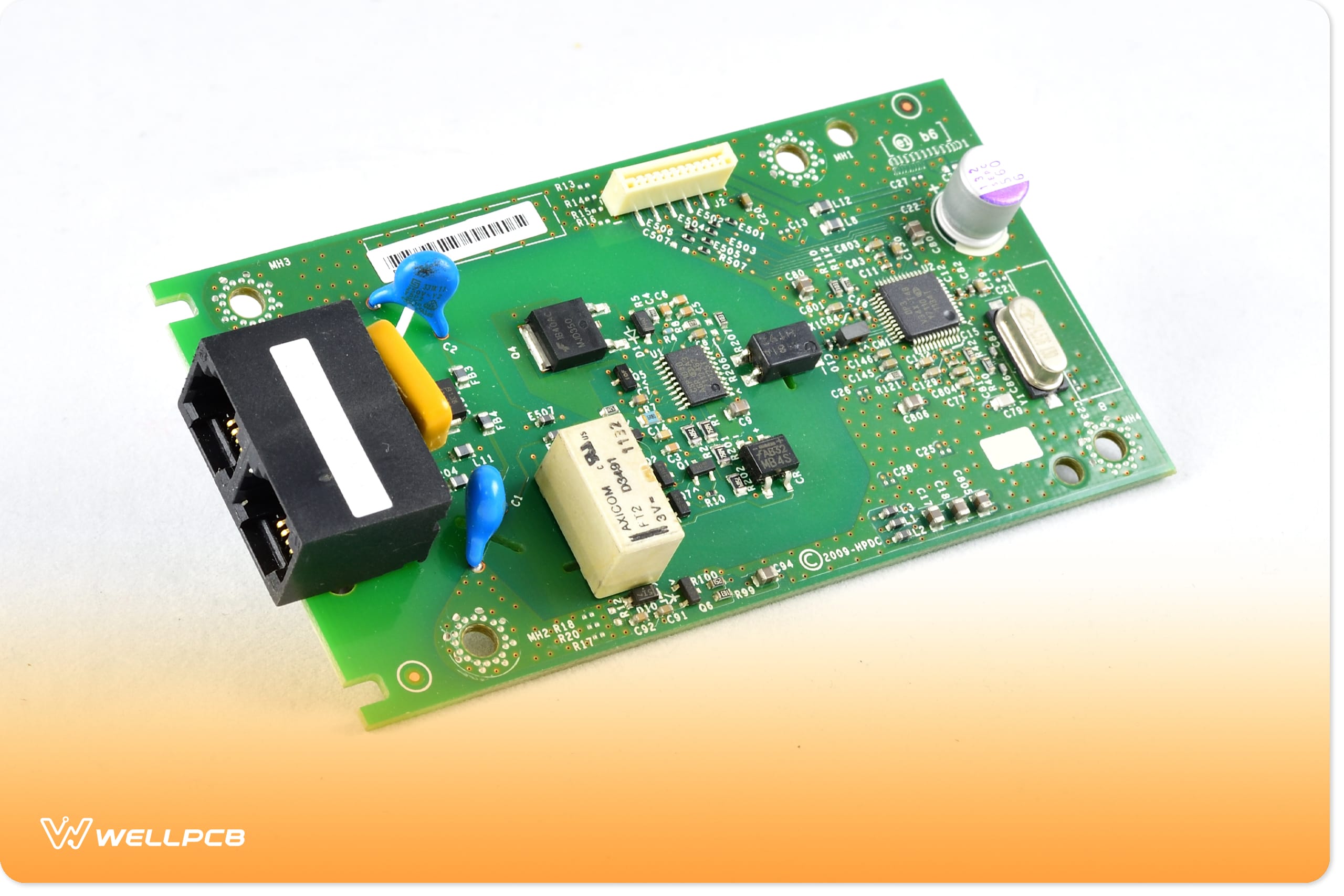
(A through-hole IC)
3. Through-hole Mounting VS Surface Mounting
As noted earlier, two types of IC packaging are common: through-hole mounting and surface mounting. The following are notable areas of comparison between the two.
Size :
Through-hole mounting a package requires large components. You’ll notice a big difference if you compare the sizes of ICs on plated-through hole PCBs and those under SMT.
SMT allows for smaller PCB size, meaning the ICs here are small and compact, unlike in plated through-hole.
If you are concerned about size when packaging your ICs, your better choice is surface mount over through-hole.
Since the surface mount is small, you can save on space also.
Component density :
Surface mounts IC packaging results in high component density, unlike through-hole packaging.
With surface mount, it’s possible to fit everything in a much smaller space while achieving functionality.
That’s not the case for through-hole, where components tend to be too large.
For example, several 14 or 16-pin dual in-line processors that measure around 0.80 inches x 0.35 inches can perfectly fit in an area of one square inch or smaller.
But on the other hand, such would be impossible would it had been plated through-hole packaging.
Assembly error correction:
At some point, errors are prone to occur regardless of the type of technology employed. When errors occur, correction or repairs may be necessary.
When looking at error correction, you can undertake quickly with plated through-hole packages.
The components are large enough for visibility and ease of repair. But such isn’t always the case with SMT.
Since the parts tend to be small and sit cl—or to each other, error correctionmeasuringcky.
Electromagnetic compatibility:
Electromagnetic compatibility is the ability of electronic components to work as desired. They should do so in their electromagnetic environment.
There’s better electromagnetic compatibility to through-hole at some point.
The reason for such is that SMT offers a shorter return path.
The correctionsturn path comes about since components sit close to each other instead of through-hole.
Cost :
Unlike SMT, through-hole packaging can save significant costs. For instance, it doesn’t require detailed and expensive equipment.
This type of mounting maysaveg circuit makers hundreds of thousands of dollars.
But when it comes to surface mount, the manufacturing costs tend to be slightly higher.
For instance, manufacturersmusto utilize a pick-and-place machine in one of the most expensive markets.

(A surface-mounted PCB)
4. Integrated Circuit Packaging Material
Electronic packaging is one of the most materials-intensive applications lately. Manufacturers need to use several materials here.
IC packaging–Types of materials:
The materials here include semiconductors, glasses, ceramics, composites, metals, and polymers. Glasses and ceramics work as insulators or dielectrics, while polymers work as conductors.
Metals, on the other hand, work as conductors in the package. Composites contain materials that can work as electrical conductors or thermal enhancements.
IC packaging–The patch material:
You will have to useit to make patches should you find yourself in such a situation. A patch is a piece of fabric that covers an undesirable opening.
Plenty of patch materials exist. Several can be used during IC packaging. However, some ideal materials are piezoelectric.
IC packaging–Sealant:
Lastly, you may often hear of a sealant when it comes to IC packaging.
But what are bonds and some of their uses?
Just as the name goes, an adhesive is a material individuals use to seal anything they want to close.
The primary function of sealants is to ensure that the sealing devices are either watertight or airtight.
Sealants are necessary during IC packaging since they ensure that water or air don’t damage the IC’s rest. You will have to use them to make patches.
For these reasons, bonds are mandatory.
Silicone sealant is one of the ideal types of adhesives. It is long-lasting and perfect for protecting the whole package from corrosion.

(IC packaging materials)
5. Assembly method of IC packaging
IC assembly electronically connects the output and input bond pads found on the IC to the corresponding bond pads on the package. In our case, the box is a system-level printed circuit board. There are several types of IC packaging that manufacturers use. Some of the most common ones include the following:
IC packaging–Dual-in-line package :
A Dual-in-line package, or DIP, is one of the most common assembly methods for IC packaging. It is an electronic device package consisting of a rectangular housing with two adjacent parallel rows of electrical connecting pins.
Take note that the box could either be through-hole-mounted to the PCB or inserted in a socket.
If you are keen enough, you’ll realize that most people refer DIP to DIPn.
Here, n refers to the total number of pins.
For example, a microcircuit package with two rows consisting of eight vertical leads would be a DIP18.
IC packaging–Small outline package :
A small outline package is another IC packing assembly method manufacturers use to achieve IC packaging, especially if they are small.
The small outline package is slightly narrower and shorter than DIPs. The side-to-side pitch is 6 mm, while the body width is 3.9 mm.
However, you must be aware that the dimensions differ depending on the package.
IC packaging–Ball grid array :
Ball grid arrays use various assemblies to provide packages with 250 to 1089 inputs and outputs. This is also one of the most common IC assembly methods.
IC packaging–Quad Flat Package :
The Quad Flat Package is an IC assembly method that many manufacturers use. Its heavy use is because it enables for one big reason.
It allows SMD ICs consisting of high interconnections to find easy use in electronic circuits. Quad flat pack integrated circuits are in several formats with pins that vary in number.

(A Dual-in-line IC packaging)
6. How Should We Choose the Type of IC Packaging?
Before proceeding, we need to stress the importance of good packaging. Integrated circuits must stay in a package to ensure smooth handling and assembly on the PCBs.
Choosing the right package is essential, as you’ll avoid cases of damage and corrosion.
So, how do you go about choosing the right type of IC packaging? Continue reading to understand.
- The number of I/Os-First, the number of I/Os matters when choosing the package. Here, BGAs are the best for their high pin counts.
- But if you are on the market for a lower pin count, the QFN package will be ideal.
- Heat management-Secondly, you need to consider matters to do with heat management. Today, the sizes of the ICs tend to be smaller but with more extensive solder masks to prevent leakage of electrical and thermal components. Be sure to discuss with your PCB supplier the capabilities.
- As such, it will avoid producing too much heat, which is why heat management matters. On the other hand, BGAs tend to display effective heat dissipation, which is why you may want to go for them.
- When choosing your IC packaging, high speeds I/Os-Third, look at matters such as High-Speed I/Os. You do not want to interfere with the package’s quality to interconnect the IC I / O signals at any time. For the best high-frequency signals, consider flip BGA.
- PCB assembly-Lastly, PCB assembly matters. Can you have the assembly of your IC package within the shortest time possible? Ensure that you factor in this factor beforehand, as not every provider can offer you what you want.

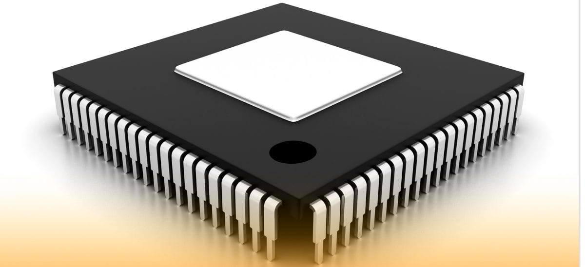
(A correctly assembled IC chip)
7. Uses and advantages of IC packaging
ICs play several essential roles in nearly all electronic circuits.
They carry out the entire data processing and calculations. IC is also one of the most critical elements of data storage.
Without ICs, an electronic circuit (such as a PCB) won’t function as intended.
IC packaging has several notable merits. For instance, it protects the component from damage and corrosion and ensures an adequate flow of current throughout the entire system.
IC packaging is also beneficial, with the package acting as a mechanism for “spreading apart” the connections from the tight pitch on the IC die. The box spreads these mechanisms to broad pitch areas that most PCB manufacturers require.

(Properly packaged ICs)
Why Is IC Packaging Important?
IC (Integrated circuit) packaging comes in over 25 variations.
The most pressing concern for IC packaging is safety and protection from external natural elements and human mistakes.
As a sensitive unit, the slightest damage to a semiconductor could render it useless. That is why the packaging comes in insulation material that is hardly affected by external impact.
Let’s explore other reasons for IC packaging.
It Increases Longevity
Integrated circuits are delicate. Therefore, dust, accidental falls, water, or scratches are likely to damage them.
Any accumulated damage will render them useless over time. The packaging keeps the material in peak condition, allowing it to last longer.
IC Packaging Material Retains Reliability
Once you have put the IC in protective packaging, you can ship out the units knowing you have sent a reliable product. Alternatively, you could use ICs knowing they’re safe for long-term use.
It Solidifies Electrical Conductivity
IC packaging doesn’t only protect the IC from physical damage. It also ensures there is no electrical interference between the IC and other components you’ll add. It ensures every pin, terminal, or lead can transmit signals without flow disruption.
Packaging Size Greatly Improves Consumer Handling
Consumer electronics are getting smaller and lighter. To that end, IC packaging helps make ICs minimalistic in everyday consumer electronics.
The end game here is that the final designs and units are highly portable and easy to handle.
Packaging Improves Heat Dissipation
We’ve already covered the effects of temperature on PCBs.
Heat dissipation affects circuit performance, durability, and reliability. Therefore, the packaging is an integral part of heat management and the overall performance of the IC.
The material used in temperature-sensitive ICs must have exceptional thermal regulation properties to be the most effective.
Package Customization Can Help In Brand Diversity
In a market awash with identical products, putting your brand on the IC packaging sets you apart from competitors.
It boosts visibility, and it can also strengthen brand trust.
Customizing the packaging to suit consumer demands also boosts mass appeal for smaller brands struggling to carve out space for themselves.
Performance Boosting
Without electronic interference, the IC and any connected components have minimal signal loss and maximum efficiency.
Overall, the ICs contribute to peak performance in any unit. The packaging ensures minimum latency and minimum power loss.
IC Packaging Design Considerations
When it comes to IC packaging design, the first three considerations are broad considerations that focus on look and functionality. While other considerations arise from specific factors, let’s address the broad considerations.
Dimensions
Of course, dimensions influence a big chunk of the design. Whether it’s for in-house manufacturing or making PCBs for a company, dimensions are a top priority in the design phase.
Mounting Style
Every IC has a unique mounting style that links it to other components.
The design phase must consider the IC’s purpose and how it fits into the PCB. For example, ICs made for hobbyists have different designs from ICs made for commercial mass usage.
Pin Count
The designs will be different if one IC has 3 pins whereas another has seven. This information will be included before the design stage starts.
Also, if an IC has pins that poke outward from the center, whereas another has pins that splay from the sides, the design will not be similar.
With those general considerations in mind, these other considerations also influence the IC packaging design.
Cost Considerations
If you’re producing IC packaging for mass use, it’s more cost effective to use plastic packaging over ceramic. However, ceramic IC packaging dissipates 48W more than plastic’s 2W. Smaller packaging usually gets hotter faster than bigger packaging. Therefore, using ceramic packaging in the design phase is more sensible, no matter the cost implication.
Mechanical Considerations
IC packaging must remain in place to withstand possible damage.
To that end, an IC package designer must decide whether they will use plastic such as ECN, ceramic, or metal.
Ceramic and metal packaging are more likely to support more pins and dissipate more heat.
Electrical Considerations
Designing with the electrical considerations in mind might be the most challenging bit.
The designer must use materials and dimensions that encourage low resistance, capacitance, and inductance.
Also, the packaging must reduce parasitic capacitance that is inevitable in electrical units.
Summary
As you’ve seen, there’s much more to IC packaging for electronics systems than you may think you know. Electronics players, both old and new, need to get a clear picture of it.
This way, it’s possible to stay abreast of new developments here.
Do you have questions concerning the various types of IC packaging or anything relating to PCBs?
Feel free to go circuit board shopping; various things might get you confused.
Whether you need a single-sided, double-sided, or any other type of PCB, you can contact us.
We take pride in providing our clients with the information they need to make informed electronic parts decisions for their businesses.