Contents
PCBs with BGA
1.1 What is a PCB BGA?
A ball grid array is a chip carrier – surface mount technology – used in integrated circuits. If you want to mount your microprocessor permanently, you should use ball grid arrays (BGA).
BGA will supply you with more ininterconnectionins compared to what you get from the flat package.
The entire bottom area of your device will be utilized rather than just the perimeter.
Further, the leads are also smaller, providing you with more performance at high speeds.
Traditional pin grid array (PGA) packages have led to the development of BGA packages. A PGA package has pins arranged in a grid pattern on one face, covering it fully or partially.
While operating, the pins send electrical signals between the printed circuit board (PCB) and the integrated circuit (IC).
Now l, et’s get to how BGA is different from PGA.
In BGA, you must place the pins with pads on the package’s bottom surface. In the beginning, you will do this by sticking small solder balls.
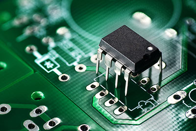
You can place these solder spheres either manually or by using automatic devices. Figure 1 shows a close-up of the ball grid array IC.
Generally, copper pads link the BGA IC and a printed circuit board (PCB). The pattern of these pads complements the solder balls.
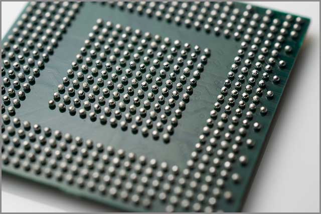
In more innovative technologies, solder balls can be placed on both the BGA package and the PCB. If you plan to develop multi-chip modules, you can use solder balls to join together different packages. Figure 2 illustrates the footprint of a BGA IC on a printed circuit board.
1.2Advantages of PCB BGA
With PCB BGA, you will get the following advantages:
1. The BGA package eliminates the issue of developing small packages for ICs with lots of pins.
Traditionally, dual-in-line and pin grid arrays surface-mount boxes had very little space between the pins.
They provided a considerable disadvantage for the soldering process with more pins. However, you will not need to worry about accidentally soldering together two pins with BGA packages.
2. Again, compared with packages with legs, the BGA package has lower thermal resistance when placed on the PCB.
That permits the heat that IC produces in the box to conduct through the PCB efficiently. Can you guess how that is a good thing?
Of course, it will save your chip from overheating.
3. What property causes unwanted sisignalistortion in high-speed electronic circuits?
The unwanted inductance in an electrical conductor is responsible for this phenomenon.
However, BGAs have very little distance between the PCB and the package, leading to lower lead inductance.
Thus, you will get top-class electrical performance with pinned devices.
4. With BGAs, you can effectively utilize your printed circuit board space. You will be able to make connections right below the surface-mount device (SMD), and the links are no longer limited to just the SMD package periphery.
5. Another advantage, though, is the reduced thickness of the package. That sounds great. You can quickly fabricate the PCBs in small electronic devices like smartphones.
6. Last but not least, you will get enhanced re-workability because of bigger pad sizes.
BGA Welding Basics
2.1 PCB BGA soldering temperature
It is crucial to carefully choose the soldering temperature and composition of the solder alloy. It would help if you ensured that your BGA PCB package solder doesn’t completely melt.
It needs to stay half-liquid, permitting every ball to lie separately from other balls.
2.2 BGA welding kit and welding machine
Luckily, BGA welding kits or welding machines are widely available in the market. You can also buy them online. Usually, the welding machines come with the following main features:
- Rework BGA and other SMDs.
- Solder, De-solder, Mount, and Remove your BGA package manually.
- Integrated with infrared heating plate and hot air heaters.
- Easy to use. It will have a touchscreen interface.
- Used to control temperature accurately
- and emergency protection.
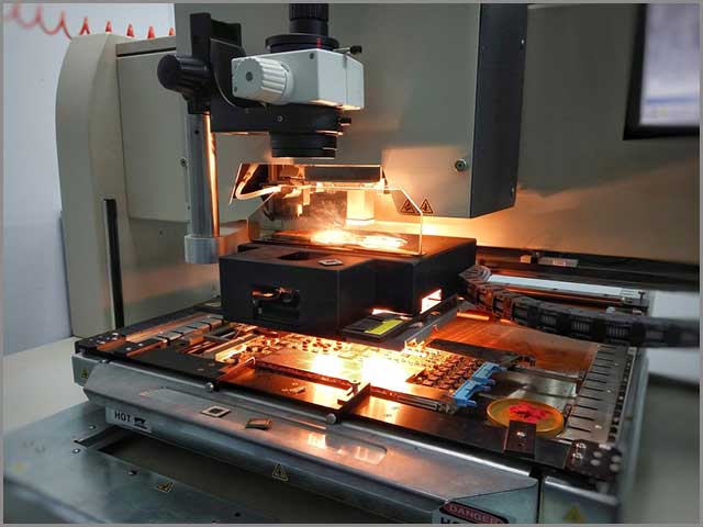
Figure 3 demonstrates a BGA welding or rework station.
In the next chapter, we will explain the BGA welding process.
In detail Welding Process
One of the significant problems with BGA initially was whether it would offer reliable welding procedures.
You don’t need to get confused with the term welding; it is just another word for soldering.
Moreover, as BGA has pads rather than pins on the bottom surface of the device, it is crucial to ensure the correct welding procedure is adopted.
You only need to ensure that the process is set up correctly. Luckily, BGA welding methods have proven more reliable than traditional quad-flat packs.
That, in turn, means that BGA assembly will also be more dependable. Thus, BGAs have been significantly used in prototype and mass-production PCB assembly.
3.1 BGA solder ball size and collapse height
While performing BGA welding, carefully choose the size of the solder balls. You will need to put a very carefully measured quantity of solder.
Further, the solder will melt when the solder balls are heated. Once melted, surface tension will allow the molten solder to align the package with the PCB correctly. The solder will then cool and solidify. Thus, your BGA PCB will be all ready.
3.2 PCB BGA assembly
PCB assembly and mass-production PCB assembly. Initially, the PCB BGA assembly was one of the major fears. Engineers were unsure whether it would achieve the reliability level of traditional SMT methods.
However, BGAs have proven to be more reliable. Therefore, BGAs have been significantly used in both prototypes. A Bill of Materials (BOM) of a PCB gets fitted onto the board.
You will need to use reflow methods to solder a BGA package.
You may wonder why that is. The main reason is that you need to ensure that solder melts beneath the BGA modules themselves.
For this purpose, the whole assembly must reach the melting temperature. Finally, only reflow methods can achieve this.
Now, many devices utilize BGA packages instead of the standard PCB BGA packages. Therefore, PCB BGA package assembly techniques are more reputable now.
Manufacturers can handle them quite comfortably.
In the same way, BGA devices should not lead to any fears when being used in a design.

BGA Package
4.1 What is a BGA package?
As we described in the first chapter, the BGA package does not use the sides of the IC for the connections.
It uses the bottom surface of the integrated circuit and thus provides more space for the links. Further, BGA uses copper pads forties rather than pins.
The copper pads have solder balls, and a complementary set of copper pads on a PCB allows them to be easily fitted on the PCB.
It is interesting to note that the places are arranged in a grid pattern under the IC. This specific arrangement gives the Ball Grid Array its name.
4.2 BGA package size
Generally, the PCB BGA packages have a pitch size of at least 0.3mm. Moreover, the length between two BGA packages is usually around 0.2 mm.
Moreover, the least distance to the circuit line is about 0.2 mm. These are the available sizes; if you need different sizes, you may contact the manufacturers.
4.3 BGA package types
There are six different kinds of BGA packages. We will go through each of them in this section.
- Moulded Array Process Ball Grid Array (MAPBGA): A BGA package with low inductance and simple surface mounting. You can use it for low-performance to medium-performance devices. It is highly reliable, cheap, and has a small footprint.
2. Plastic Ball Grid Array (PBGA): Again, this BGA package provides low inductance, simple surface mounting, high reliability, and cheap. Further, its substrate has more copper layers, allowing the handling of more heat dissipation levels. You can use it for medium-performance to high-performance devices.
3. Thermally Enhanced Plastic Ball Grid Array (TEPBGA): As its name suggests, this BGA package can handle significant heat dissipation. Its substrate has solid copper planes.
4. Tape Ball Grid Array (TBGA): This BGA package is a solution for medium—to high-end applications. It provides exceptional thermal performance and does not require an external heatsink.
5. Package on Package (PoP): Do you want to save space on your PCB? If so, you should use this BGA package. It permits you to put a memory device on a base device.
Micro BGA: This BGA package is relatively small compared to standard BGA packages. The industry’s predominant pitch sizes are 0.65, 0.75, and 0.8 mm.
Designing PCB BGA
You may encounter challenges while designing PCB BGAs. This chapter describes two strategies that will help.
5.1 Define Appropriate Exit Routes
You may be having problems creating appropriate exit routes that don’t result in assembly failures or similar issues.
For the right fan-out routing plan, you need to consider many PCB specifics, such as the number of I/O pins, pad and via size, trace width spacing, and the number of layers needed to fan out the BGA.
5.2 PCB BGA—Determining the Needed Layers
As a designer, it will not be easy to decide the number of layers of a PCB layout. A PCB with more layers will be expensive. On the other hand, you may need to increase the number of layers to reduce noise.
First, you should determine the size of the via and the space and trace width of the PCB design. Then, you must decide on the quantity of single-channel traces.
After that, you should determine the number of layers that are required. For fewer layers, the critical point is to reduce the application of I/O pins.
In the end, we agree that designing a BGA is not easy. You will need to follow specific design rules.
As a beginner, you may find it challenging, but Altium Designer will surely make it easy for you.
Repairing Ball Grid Array
Replacing BGA with a new one is possible. You can repair or refurbish the BGA after removing it. It will come in handy if your chip is expensive.
The BGA repairing process is also called BGA rebelling. In this process, solder balls are replaced. In the market, you can buy tiny, ready-made solder balls. They are specially designed for this purpose.
6.1 PCB BGA—BGA inspection
BGA devices have a significant issue in that optical methods cannot view the soldered joints. Therefore, you cannot check the connections by only testing their electrical performance.
The relationship may be soldered inadequately, and with time, it deteriorates. Thus, there is only one reliable method of inspection: X-ray inspection.
X-ray inspection will see through the soldered connections beneath the device.
However, work has shown that BGA packages will solder without any problem if a solder machine is configured correctly.
It would help to ensure the heat profile is set up correctly.
6.2 PCB BGA—BGA rework
By now, you can predict that reworking PCB BGAs is also not easy. However, with the right equipment, you can do it perfectly.
In the PCB BGA correct procedure, a specific rework station provides the heat required for removing BGA.
That includes a thermocouple to control the temperature, a tool-holding with an infrared heater, and a package-lifting vacuum device.
You must proceed carefully and ensure you are only heating and removing BGA. Moreover, nearby devices should be affected as little as possible. Otherwise, they will get burned.
PCB BGA–Conclusion
In this article, we have explained in detail how PCB BGAs can be the perfect surface-mount technology for your ICs.
What problems you may encounter and how to deal with them. You don’t need to visit any other website for any details.
However, if you still have any questions, contact us at [email protected]. Our team of engineers will be more than happy to answer them.