Contents
Attiny84 Pin Configuration
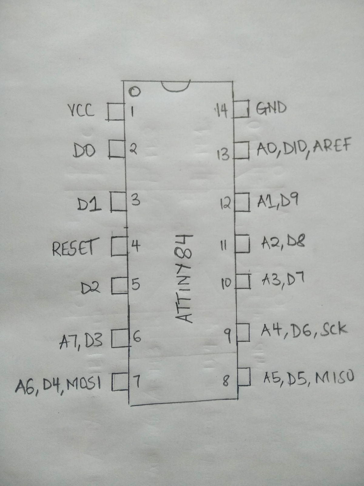
(Schematic diagram for Attiny 84 pinout.)
Left Set Pins(1-7)
- Pin 1- VCC. It is the positive pin of the MCU.
- Pin 2- PB0(PCINT8/XTAL1/CLK1).
- The Pin 2 connects to side B of bit 0/oscillator pin from the clock coming from an external source.
- Pin 3- PB1(PCINT9/XTAL2).
This pin leads Port B with bit 1/ oscillator pin/pin change interrupt, source 9.
- Pin4- PB3(PCINT11/RESET).
Pin 4 connects to port B with the bit 3/reset pin. Mainly used for debugging and programming. Also, it is a source 11-pin change interrupt.
- Pin 5- PB2(PCINT10/CKOUT/OC0A/INT0).
Pin 5 is an input and output pin of the B port. Additionally, it has a 2 bit or system clock out and an external interrupt 0/timer.
- Pin 6- PA7(PCINT7/ADC7/OC0B/ICP).
It is a bidirectional input and output pin of the A with a 7-bit. Also, it is the input channel 7 of the ADC. A timer compares match Bout/Timer 1 capture/ pin interrupt change 0 from source 7.
- Pin 7- PA6(PCINT/OC1A/SDA/MOSI/ADC6/D0).
During the ICSP programming, an ADC input channel6 (pin interrupt) changes 0 from source 6/SPI MOSI. Pin 7 is an input/output pin with a 6 bit. A USI data input/counter 1 compare match A out.
(a photo showing a microcontroller with eight pins.)
Right Set Pins(8-14)
- Pin 8- PA5(MISO/PCINT5/ADC5/D0/OC1B).
It is a bidirectional input and output pin of A with a 5 bit. A USI data output/counter 1 compared with B-out matching. Similarly, during ICSP programming, an ADC input channel 5 (pin interrupt) changes 0 from source 5/SPI MISO.
- Pin 9- PA4(USCK/SCL/SCK/PCINT4/T1/ADC4)
Pin 9 is a bidirectional input and output A pin with a 4-bit. It operates using an ADC input channel 4. A three-wire USI clock is necessary for ICSP programming. The counter1 clock source/I2C SCL/ pin interrupt changes 0 from source 3.
- Pin 10- PA3 (T0/ADC3/PCINT3)
It is a bidirectional input and output pin of A with a 3 bit. AN ADC input channel 3/counter0 clock source/ pin interrupt changes 0 from source 3.
- Pin 12- PA2(AIN1/ADC2/PCINT2)
Pin 12 is the input and output pin of the A port with a 2-bit. An analog comparator – input/ADC input channel 2/ pin interrupt changes 0, from source 2.
- Pin 13- PA1(AIN0/ADC1/PCINT1)
It is the input and output pin of the A port with a 1 bit. An analog comparator + input/ADC input channel 1/ pin interrupt changes 0, from source 1.
- Pin 14-PA0(AREF/ADC0/PCINT0)
Finally, pin 14 is the input and output pin of the A port with a 0 bit. An ADC input channel 0/external analog reference voltage/ pin interrupt changes 0 from source 0.
(a microchip with visible gears.)
What is Attiny84?
Attiny84 is a compact size 8-bit Microcontroller – MCU with an AVR RISC architecture. This architecture is based on the property that the microcontroller has 14 pins. Notably, 12 pins are input/output pins. Moreover, the architecture contains a packaged microchip picoPower technology that plays a significant role in the device’s high performance.
Attiny84 has a robust instruction architecture. It gives a processing speed of 1MIPS/MHz. Therefore the device simultaneously balances the power consumption while processing a high-speed performance.
(a computer microcontroller.)
Attiny84 Features and Specifications
- Firstly, attiny84 has an 8-bit AVR CPU architecture and consists of a single 8-bit and 16-bit timer module.
- Second, it works with a minimum operating voltage of 1.8v and a maximum (V) of 5.5.
- Thirdly, the device has a 10-bit, equivalent to an 8-channel ADC module, and 14 pins (12 being I/O pins).
- Also, attiny84 has a memory configuration with 8kb program memory and 0.5kb RAM bytes.
- Additionally, attiny84 is a product type that lacks a DAC module with only 1 SPI and 1 I2C communication protocol.
- Moreover, attiny84 contains an external oscillator and an 8MHz internal oscillator for the functional safety of the microcontroller.
- Lastly, it has a 20MIPS CPU speed with a 512bytes data EEPROM, being an excellent product with only one comparator.
Attiny84 Alternatives
The perfect alternative to attiny84 is the attiny2313A. However, the other alternative products include; attiny48, attiny417, attiny28L, attiny88PA. Notably, atmega8A, atmega8535, atmega6490, atmega8515, and atmega645A are similar to the attiny84 features.
Attiny84 Programming Tutorial and Steps
Materials needed
The required hardware equipment includes;
- LED
- 470-Ohm resistor
- Breadboard
- Jumper wires
- Attiny84
- Arduino Uno
Steps and procedures
You need to follow a few steps to set up and program your attiny84.
- First, collect all the necessary hardware interfaces.
You can easily purchase them or reuse others from your old projects.
- Second, add a core Attiny support to the Arduino Uno IDE.
Notably, when you get to step 2, an option referred to as the processor, you should click on attiny84. Also, sometimes, you may not have the correct socket to plug the attiny84. So, you will need to make a socket out of jumpers. This process only depends on the programmer or Arduino board you are using as an ISP.
- Finally, configure the Arduino to serve as a common software.
Next, you will connect the VCC, GND, MISO, MOSI, RST, and SCK pins to the necessary connectors. Once you have successfully connected via the USB, you should open up Blink Sketch on the Arduino IDE.
Now, change LED_BUILTIN to 0, then press CTRL+U to upload. This change is necessary because the attiny84 lacks LED wiring. This procedure should make your program upload successful. If not, select Tools and click USBtiny ISP as the programmer.
These three steps should not give you a hard time at all.
Code;
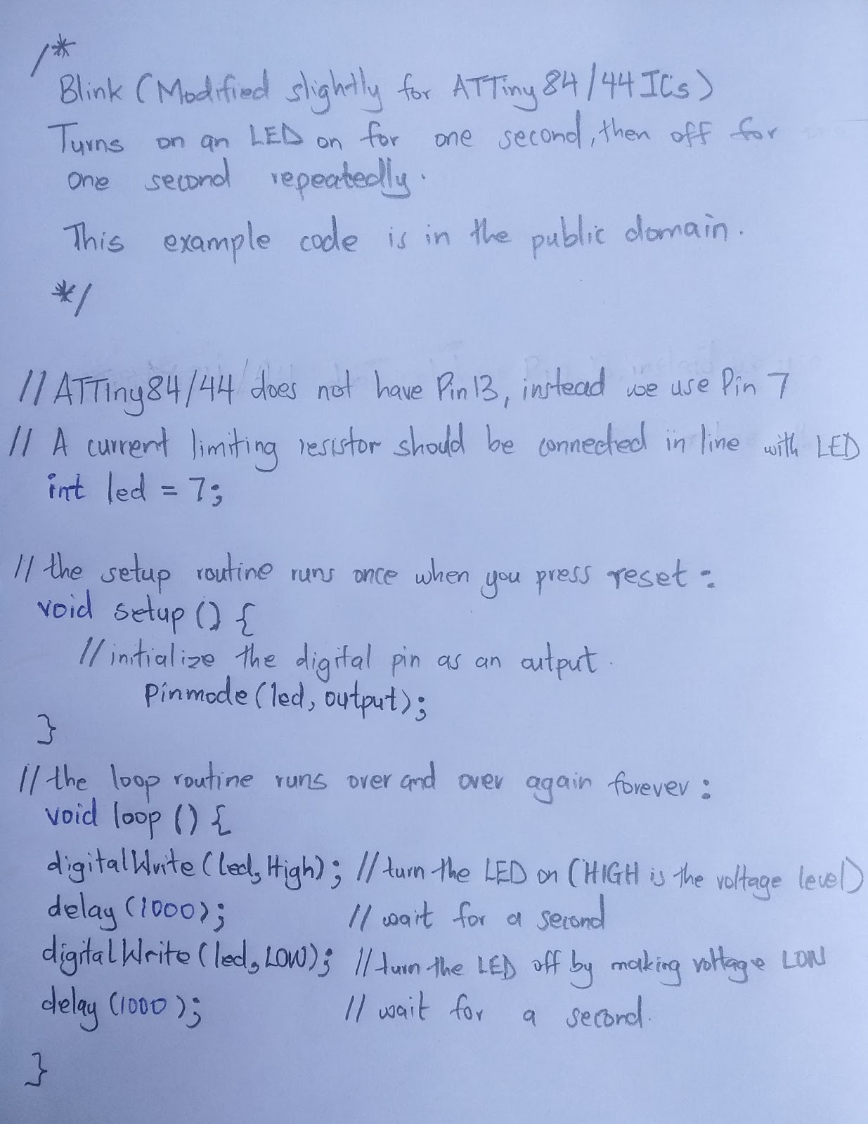
(The code that you need to run.)
Notably, just like any other program, you must check its working. To perform this check, you will connect an LED further down to the ground and pin 0. Also, ensure you involve an accurate resistor and notice the LED glowing. Otherwise, check your connection and program code to ensure everything is fine.
(DIY electronic project with microcontroller and other electrical components.)
Summary.
Happy building! We hope this article helps you answer attiny84 questions. For more information regarding this or any of our articles, please do not hesitate to contact us.