Contents
What is PCB Programming?
Most modern PCBs feature integrated circuitry of some sort.
These chip packages (or ICs) and microcontrollers allow engineers and technicians to program the PCB to function in the electronic device it will eventually integrate into.
Modern-day fridges, washing machines, and microwaves are all everyday appliances that use firmware to operate in one capacity or another.
Of course, slightly more complex devices, such as single-board computers (SBCs), require more advanced firmware and software.
Nevertheless, regardless of the complexity of the device or its firmware, manufacturers and technicians must be able to embed the firmware on the PCB.
This is where PCB programming comes in.
It typically refers to uploading or flashing coded instructions or firmware onto a PCB during assembly or manufacturing.
However, it can also refer to planning and designing the layout of the PCB and its components, as well as testing and debugging the PCB.
Ultimately, we could consider any PCB manufacturing or assembly process part involving firmware or software as PCB programming.
However, this guide will focus on PCB programming for component functionality and testing.
PCB Programming Methods
There are three main PCB programming techniques:
On-board Programming (OBP)
On-board programming describes the direct programming of a PCB’s microcontrolMicrocontrollerdevice. Manufacturers and technicians can perform it during or after the assembly process.
Since an external programmer isn’t necessary, OBP can reduce manufacturing time and streamline inventory management.
Manufacturers don’t have to mount and dismount PCBs to program them. Moreover, they can directly modify and update data on the PCB if necessary.
Stand-Alone Programming
Stand-alone programming allows manufacturers to program individual components before mounting them onto a PCB. Hence, it is also often referred to as off-board or universal programming.
Stand-alone programming allows manufacturers to test and ensure that each component is fully functional and working correctly before connecting it to the rest of the assembly. This PCB programming technique is advantageous because it’s more flexible, cost-effective, and reliable than other testing methods.
In-Circuit Testing
As the name implies, manufacturers use this method to (mainly) program PCBs for testing or to perform PCB-related tests. As with stand-alone programming, in-circuit testing is performed on the component level.
Most ICT systems use probes, with the “bed-of-nails” type being one of the most well-known. ICT systems are popular among manufacturers because of their high test and fault coverage, speed, efficiency, and convenience.
PCB Programming and Design Software
As we previously mentioned, PCB programming is a broad term. It can refer to coding or programming for the design, fabrication, and testing phases.
Consequently, each phase requires its specialized tool or software. The most popular tools for each process are as follows:
Programming Software
Manufacturers, technicians, and hobbyists use the following tools to upload software to microcontrollers (mainly).
- Microchip MPLAB X IDE
- STM32CubeProgrammer
- Arduino IDE
- MIDE-51 Studio
- KtechLab
Design and Layout
PCB Manufacturers and designers use the following CAD applications to create and automate PCB schematics and layouts:
You can also use the above design and layout software to verify and refine your PCB designs.
They include Design for Manufacturability (DFM) features that ensure your designs are ready for fabrication. In addition to these capabilities, they can also allow you to simulate tests and virtually debug your PCBs.
However, design and testing software is only a fraction of the equation. If you want to fully and comprehensively test your PCB, there are a few other hardware-based tools you should be privy to…
Other PCB Programming and Testing Tools
Other hardware tools and instruments that you can use to test and debug your PCBs include:
- In-Circuit Debuggers (ICDs)
- Multimeters
- Logic analyzers
- Oscilloscopes
- In-System Programming Adapters
- Test Points and Probes
- JTAG Boundary Scanning Tools
- Automated Test Equipment
- Functional Test Systems
- Bed-of-Nails Testers
System Design
1. System / Preliminary Design
In PCB Programming, the primary focus should be understanding the board’s overall design before you begin when you know what component fits where the design process gets much more comfortable.
The preliminary design comprises two significant steps. First, you should build a diagram of the complete system. Treat this as your design blueprint.
The blueprint will guide you through the inputs and outputs without going into too many details.
It is to understand how the entire board functions and connects.

2. Block Diagram
A block diagram includes one block for every significant component cluster, showing how these modules are linked, how they interact, and how much voltage flows through each stage.
When all of these blocks are added to the diagram, add these details to the picture, including how much initial energy will be required.
It will make your job easier by showing if you need any voltage controllers for shifting for every core block.
Shifters are best for voltage control because two electrical parts are linked through contributor voltage. Shifters are also best when these two electrical parts use different energy levels.
3. Select MicrocontrolMicrocontroller
You can decide what kind of microcontrolMicrocontrollerd on necessary details like cost, availability, properties, etc. You can get all these details from the distributor’s site.
Price over performance –Arm Cortex-M is a quality MC because of how cheap they are and the level of performance you can get out of them.
Even if you are PCB programming for only 8-bit, you can afford and should use a 32-bit Cortex-M.
Performance – depending on the number of GPIO pins and which uses the serial protocol.
The simplest and cheapest microcontrollers have 32 pins with different features. The top-of-the-line has up to 216 pins; however, this might be too complex for a beginner.
Leaded Package – This is an excellent feature because the pins of the microcontrolMicrocontrollerily available.
The packages that come without being led have the pins tucked below the container. It means it is challenging to reach the nails if you don’t have any test points available.
PCB Programming– Schematic Circuit Design
The connector includes a regulator to control voltage, an MC chip, and a PCB programming connector.

4. Capacitors
To do this, we will follow these steps.
1. Begin the design by positioning a capacitor over the input pin on the regulator. Place another capacitor on the output pin of the regulator.
The first is for the input voltage, and the second is for saving charge to pass it to impermanent loads.
The second capacitor also acts to stabilize the regulator. Without this, the regulator will fluctuate.
2. You will place capacitors for decoupling near the MC’s supply pins. You can consult experts to determine what capacitor to use for this function.
5. Microcontroller Pinout
Microcontroller manufacturers usually configure many different functions on the same pin to reduce the total number of required fasteners.
In the beginning, the nail will be used automatically. However, these pins can also have alternative functions. Make sure that no two services need to be assigned to a pin.
6. RC Oscillators
The clock is necessary because it determines that the microcontrolMicrocontrollere functions in proper sequence at every second.
Some microcontrollers with pre-installed clocks watch timers, also called RC oscillators, because they combine the timing of both a capacitor and a resistor.
The downside is that they have lower precision. Temperature can majorly affect the level of oscillation accuracy.
For starter kits, they are excellent. But these clocks are not advised if you are designing something that needs extreme timing accuracy.

7. Programming Connector
There are only two programming protocols: the JTAG and Serial Wire Debug.
The SWD only needs five pins to perform clock, i/o, ground, contributor voltage, and reset.
This can be the ideal choice if you want to design a small board.
JTAG connectors can have many pins and are suitable for complex programming.
8. Power
The microcontrolMicrocontrollertributor voltage to control the components. For this purpose, you can use an external USB charger.
Calculate the output voltage that feeds into the regulator and the stable output to decide what supply suits your design. One GPIO pin needs around 24 mA of current, so calculate the source current based on that.
For basic models, the microcontrolMicrocontroller up to 300 mA with ease.

9. Electrical Rules Check
With the help of colored checks, you can add some errors for pins. This will instantly tell you if there are any issues with the board and where that is originating.
The last step is to check that you don’t have any short circuits within bets, pins touching each other, or any pin remaining unconnected.
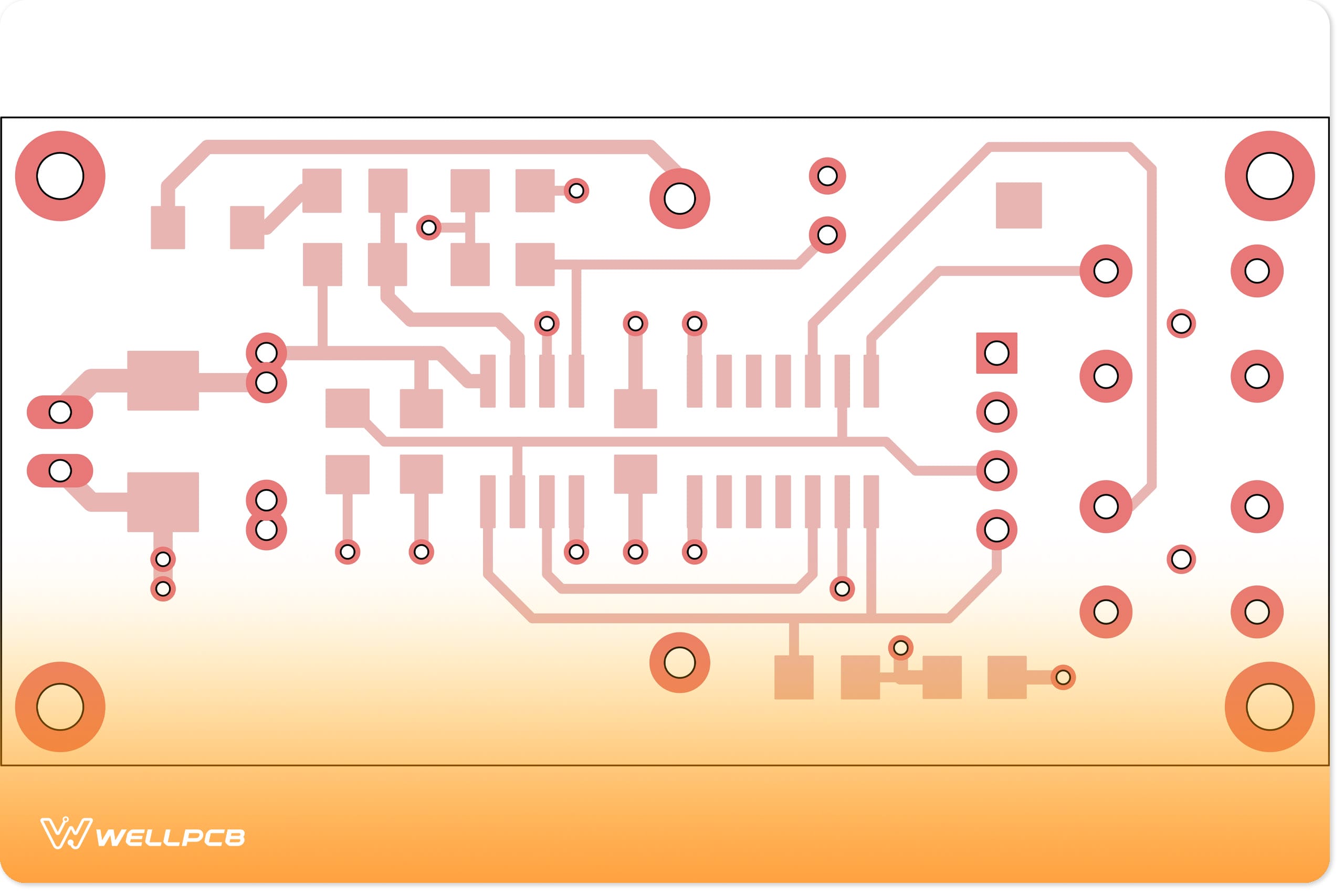
PCB Layout Design
In this step, you can start placing all the components inside the circuit board design. Then, you can use ‘convert to PCB’ to ensure the design creates the finalized product with every component in place.
10. Component Placement
This step can check the correct positioning of the parts. If you are using software for PCB design, you can already place components. However, experts like doing it manually for better layout performance.
Ensure the regulator positions the micro USB connector and the output is close to the input pin. Then, you can post the connector for programming in a place that fits the design.
After everything is in place, you can post the resistors, inductors, and the various capacitors we discussed.

11. PCB Layer Stack
The PCB is a collection of layers stacked over one another. When you have sheets capable of conduction, they need insulation material between them.
You can have a maximum of two of these, preferably on the outside. You can add more conductive layers in even numbers as you advance the designs.
12. PCB Wiring
The wiring is generally carried out after component placement. It can be done automatically or manually, but the automatic process is inefficient.
The main principle of routing is to shorten the height of the traces. It would help if you also lessened the number of vias you use and any 90-degree turns.
The higher the power of the evidence, the more critical these principles become.
You can use it through vias if you are trying to reduce the cost of building a prototype. The blind and buried vias tend to be much pricier.
The traces should also handle the current flow, or it will melt and cause the board to become damaged.
13. Verification
In the verification, you must ensure that the design rules and schema have been verified.
The DR check will ensure that you have used the right trace width, adequate space between marks, and the correct gap between the board and the evidence.
The Drs depend on what circuit board you are designing. So, it would help to have the right rules before starting the design.
14. Generating Gerbers
After completing verification, you must convert the circuit board design to the standard industry format known as Gerber.
In this format, every layer in the circuit board will have outputs in different files. The layers are silk, assembly, solder mask, and paste.
You will also need to create a file with the components’ positioning details. The manufacturer will use this file to operate the automatic component placer.
You can send these files to the manufacturer of your choice.

Summary
We analyze the PCB design process through custom microcontroller programming. We gave a brief introduction to the process to ensure that you can follow the steps.
You can contact us on time for more questions about PCB programming.
WellPCB has ten years of WellPCB will provide you with quality service and professional technology.