Contents
PCB Flaws In A Nutshell
A Billion Dollar Mistakes That Could Have Been Avoided
In 2014, General Motors spent nearly USD 4.1 billion to repair and compensate for a defect in the circuit of one of their car model’s ignition switches. A seemingly minor oversight in PCB manufacturing led to this colossal financial loss.
Consider the scale: a tiny component within a complex machine. Yet, a single flaw in a PCB can compromise the entire system. This underscores the critical role of precision PCB manufacturing in ensuring product reliability and safety.
To learn more about how our expertise in PCB manufacturing can help you avoid costly mistakes, click here: manufacturing PCBs
Was the case of General Motors an isolated case?
No. About a year ago, Samsung spent nearly $5.3 billion to take back and compensate for a defect in the Samsung Note seven smartphone’s charging system. So yet not Samsung alone; 33 million McDonald’s fitness bands were recalled about the same time (the cost was never disclosed).
Generally, stories of PCB defects that cost billions of money to repair are becoming the bread and butter of modern electronic design stories.
Startups do them just as much as established companies do them.
The bitter truth is that these mistakes aren’t pardonable by the market. So, how will you know when a PCB has defects?
PCB Testing Stages And Indicators Of Poorly Tested PCBs
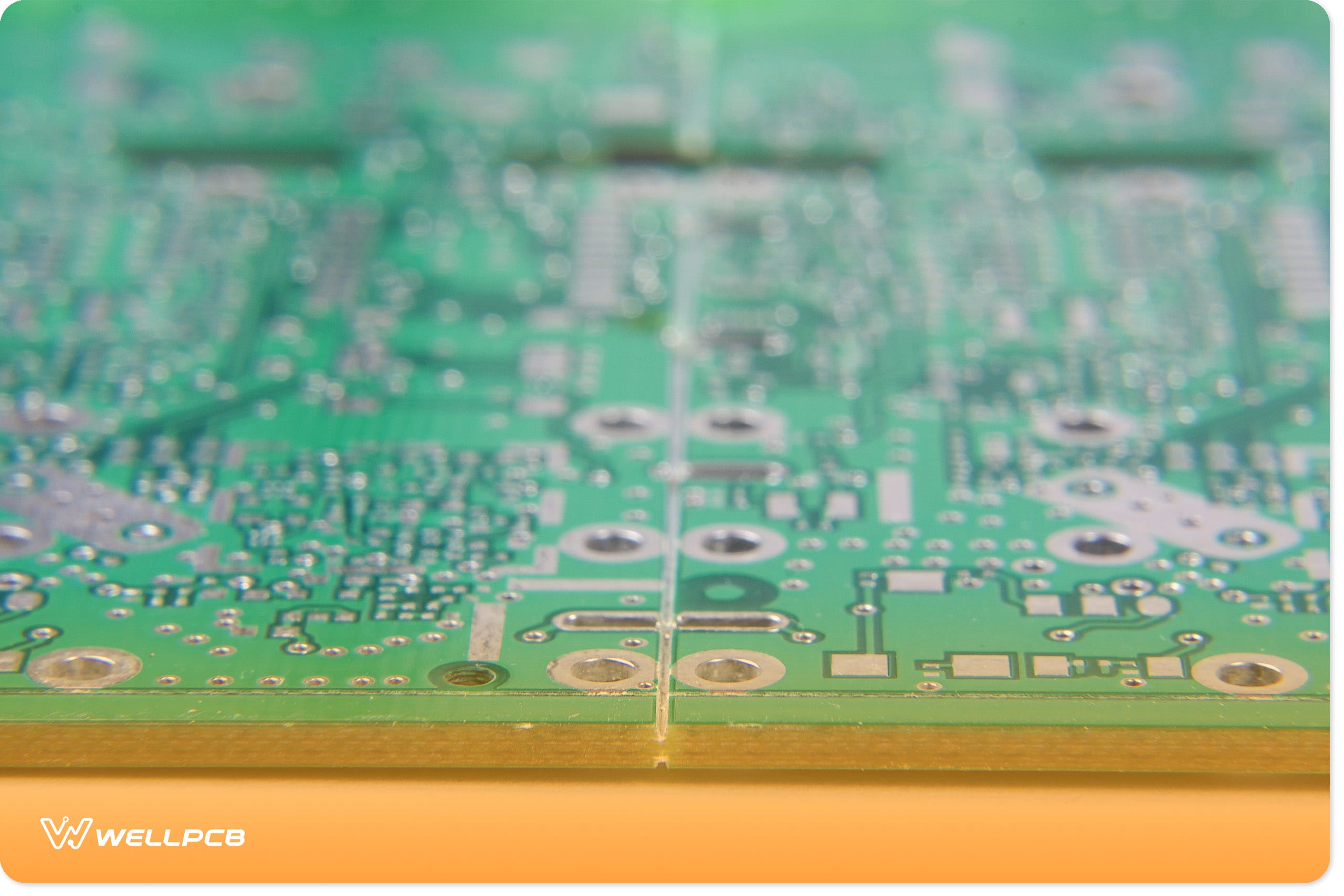
Sometimes, it is effortless to detect faults in PCBs. For instance, by visually inspecting a PCB, you can notice common defects like brown-colored overheated joints.
Solder joints with too much solder, insufficient wetting, and unstable components with disturbed joints (you can read more about these defects in cold solder joints).
This method of detecting defects is called Manual Visual Inspection (VMI).
To increase accuracy in VMI, you might want to use a hand lens to check through the joints and ensure no openings on the joints.
You can do this inspection by checking for light penetration at the joints with the aid of a lens.
However, eyes might sometimes cause PCB defects that can affect PCB efficiency.
Most such defects are only notable through testing the effectiveness of the device components. Such extended evaluation requires improved and specialized equipment.
It is also done under rigorous variables assessments like currency, voltage, capacitance, and resistance. These variables, too, could dictate the use of other specialized equipment, as we shall discuss in later chapters.
By comparing the expected input and output on various components against the actual measurements.
You can be able to know if a few parts of the board are defective.
This process is known as In-Circuit Testing (ICT). ICT becomes complicated when more components are used in a circuit.
Because of these complications, computerized equipment has been developed to ease testing individual PCB components.
Most of these devices will be discussed later as well.
The last indicator of a poorly tested PCB is an increase in customer complaints. Now, primarily, all devices attract terrible reviews from users.
It is very typical. Some customers may criticize a physical design, a feature, or anything else.
However, when complaints about a particular electronic persist over its efficiency or performance, that could indicate a PCB defect.
Such PCB flaws are undesirable, hardest to detect, and most expensive to organizations. They rarely occur.
When they happen, they have the most significant impact on the affected companies.
Now, look at the two common defects available in circuit boards.
Types of PCB Faults
There are two main types of PCB defects: structural and electrical. Almost al l flaws in PCBs can be classified as falling into either of these categories.
Structural PCB Faults
Structural PCB defects result from errors associated with the inappropriate structuring of a PCB when manufacturing PCBs.
These faults are the most common types of flaws in PCBs. They include defects like:
• Open circuits: As the name suggests, these are incomplete circuits that are overlooked during manufacturing. Most open circuits are solder-related and occur during soldering, often resulting from not melting the solder appropriately.
These errors have the highest preference of happening in PCBs, with a 25% occurrence rate.
• Insufficient solder: these defects are also solder-related.
However, they often occur due to insufficient wetting of a joint. Inadequate solder defects have an occurrence preference rate of 18%
• Short-circuiting: even though short-circuiting can be classified in both structure and electrical defects, short-circuiting has a higher preference rate of occurring due to a wrong design than a result of a defective electrical component. The fault occurs at a rate of about 13% in the overall PCB defects.
• Missing electrical component: these errors occur with a preference rate close to that of short-circuiting (about 12%).
• Misaligned components: Misaligned components can sometimes be noted after designing but just before assembly. These defects occur at a rate of about 8% of the overall number of defects during production.
• Excess solder: even though excess solder can be problematic, extra solder causes defects that are rarely produced.
This argument is correct because excess solder is easy to notice and rectify. However, there are times when these defects occur. These errors occur at a rate of about three percent.
• Missing nonelectrical parts: These errors hardly occur. They have a meager preference rate of occurring of about two percent.
Electrical Defects
Electrical defects are flaws that stem from the wrongful use of electrical components in circuit boards. These errors rarely occur in modern times, and even when they do occur, they are not as fatal as design errors.
• Defective electrical components: these defects occur when defective components are soldered onto circuits.
They are also easy to detect and rectify. These errors have a preference occurrence rate of about eight percent.
• Using wrong components: Sometimes, defects can occur when faulty components, e.g., resistors with different ratings than the recommended ratings, are used. They occur at a rate of about five percent.
• A wrong orientation of components: these defects occur when components are soldered with incorrect exposures. They occur at a rate of about two percent.
Chapter Overview
Comprehensive testing of PCBs is often implicated in the quality of electronics a manufacturer produces.
Well-tested PCBs, where testing is done with an eye to detail, result in high-quality electronics, just as poorly tested PCBs result in flawed electronics.
As you might have observed from the few illustrations, PCB flaws are always expensive. To startups, PCB blunders could cost a company its reputation.
To developed companies, defects could cost them money and part of their reputation. Both the two losses are undesirable.
In the olden days, many emphases were paid to the errors that could be done at the designing phase of PCBs.
However, with improved technology, there is an improvement in the design of PCBs nowadays.
More emphasis on PCB testing has been taken on manufacturing PCBs itself.
That is why any electronics manufacturing company interested in staying in the market for a longer period must invest more in testing PCBs.
In the future, we will be able to examine more closely the popular testing methods and industrial equipment that can be utilized to test PCBs.
PCB Testing Methods
When developing local PCBs as a hobbyist, you might not need any consistent strategy to establish the PCBs. Consequently, you will not require a testing strategy either.
Everything can fall into place once you have a rough sketch of the circuit you expect.
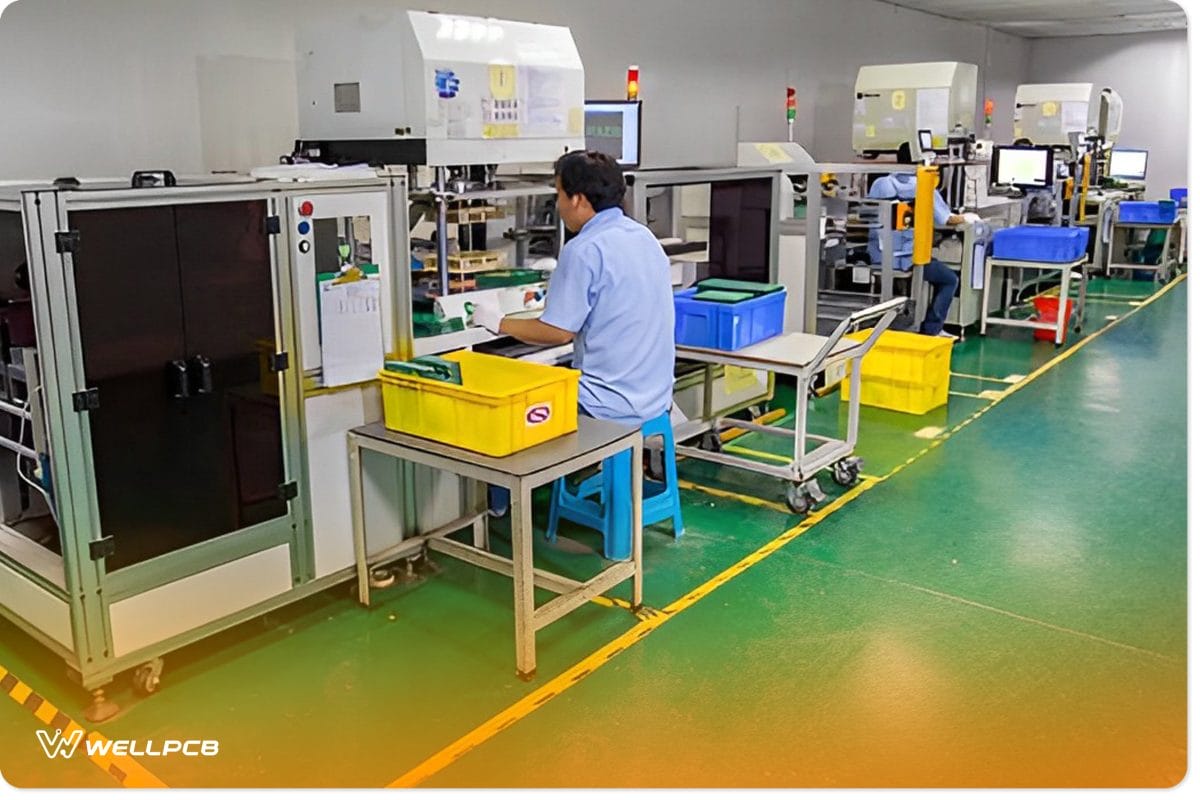
However, commercial PCB production and testing do not gamble in their implementation procedures. They follow strategies that aid the evaluation of efficiency and tolerance to faults. Currently, there are about seven approaches to testing PCBs.
Only three of the seven are dominant in the industry. These three top categories of testing include Manual Visual Inspection (VMI), In-Circuit Testing (ICT), and Functional Testing (FT).
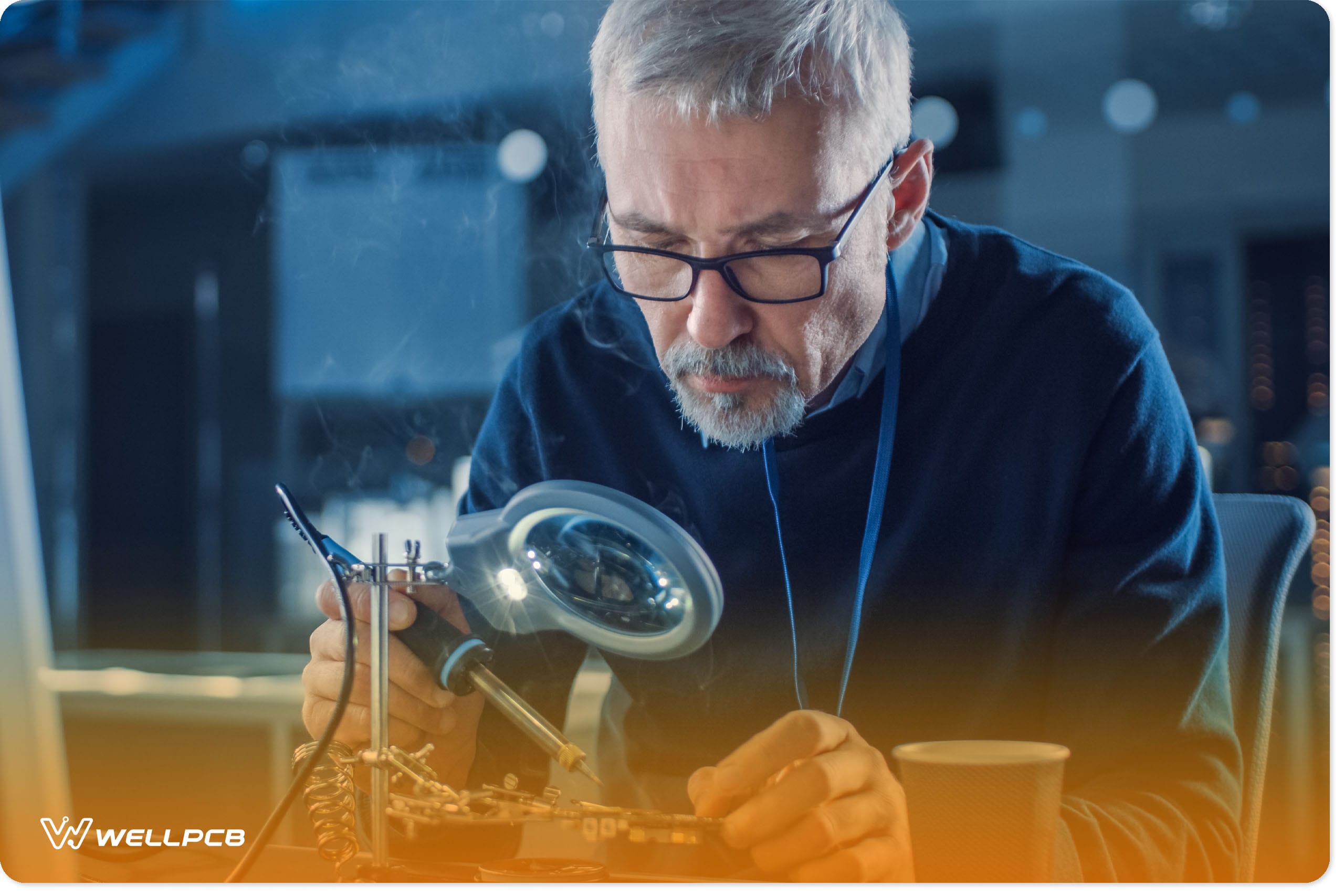
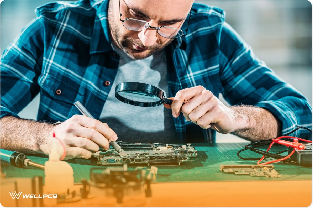
PCB Testing—Manual Visual Inspection (MVI)
That is the primary method of testing PCBs. It involves looking for faults in a PCB with an unaided eye. VMI is the simplest, oldest, and still the most popular way of inspecting PCBs.
It is applicable for the simple, low-volume production of PCBs.
However, it is not very efficient for high-volume or complex PCBs, as human eyes (unaided) might not notice some of the hidden connections.
Also, when inspecting high-volume productions, humans might tend to get bored or tired.
Because of VMI’s two main drawbacks, there are other methods to minimize errors, even though they are closely related to VMI. Top on this list is the use of lenses.
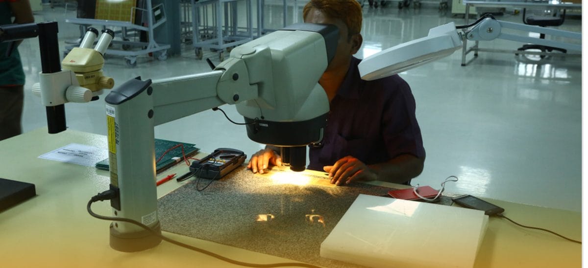
Using Microscopes And Lenses
Your PCB might fail to meet its design requirements even though unaided VMI might show that all is well. This is when you will need a closer view through a lens or a microscope.
Sometimes our eyes might not be so effective in detecting some minor defects in the solder joints of PCBs.
However, with the aid of lenses, you can magnify the boards and bring the connections on the board to a closer examination.
Using X-Rays
X-ray scans on PCBs give many details about a board that cannot easily be seen even under a lens. X-rays are essential when examining boards that have hidden connections.
You will need to take a few scans of the same board from different angles and then compare the images with the expected links from the original design specifications.
The only problem with using X-rays is that they are expensive, and they may not be suitable for hobbyists and small-scale producers.
Using A Saw
Surely, slicing through a board is indeed a bad idea. However, there are times when a PCB might indicate questionable connections in hidden parts (often after analyzing an X-ray image).
One of the easiest ways to settle the worries is to slice through the board with a saw and inspect the underlying connections of the faults.
In so doing, you can observe internal errors and rectify them to produce other boards better.
Automated Optical Inspection (AOI)
When producing large numbers of PCBs, VMI becomes tedious. OI is an automated improvement of VMI.
Systems take snapshots of various parts of the board and use the images to construct a representation of the actual board on a comp, which is then compared with the original design.
AOI is faster and more accurate than VMI.
However, it is expensive to acquire and maintain for simple projects.
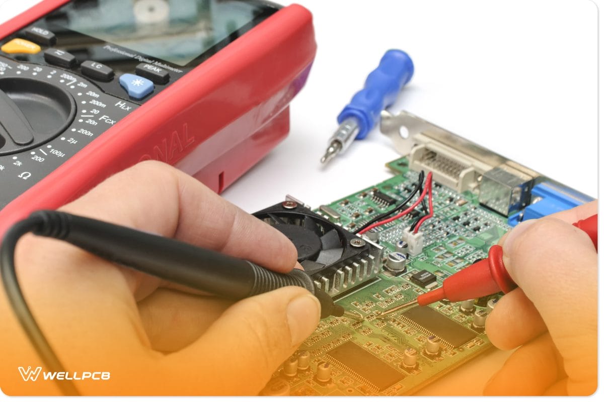
In-Circuit Testing (ICT)
In-circuit testing is the most comprehensive way of testing a PCB for defects. t aims to test the board’s components to ascertain their efficiency throughout the prototype board.
Usually, the PCB to be tested is subjected to a bed of nails connected to different components selectively to assess their performance as units.
Though it is the most recommendable way of testing, ICT is often expensive, tedious, and time-consuming.
Thus, it is usually reserved for testing large-scale PCBs. A different and newer version of ICT testing that is cheaper and offers a more economical way to test prototypes is known as the “flying probe” method, which is discussed in detail in Chapter 3 when discussing tools.
Functional testing
It is always the last phase of testing PCBs. Once a PCB is made, a functional test comprises a set of programs uploaded onto the test device to see if it performs its functions as expected.
Conclusion
These methods are not perfect; they are just less prone to errors. His assumption is valid because the strategies have been inspected and reviewed to improve their effectiveness.
These methods (to a great extent) also dictate the types of tools developed for testing PCBs. The next chapter will focus on the different industry tools for testing PCBs.
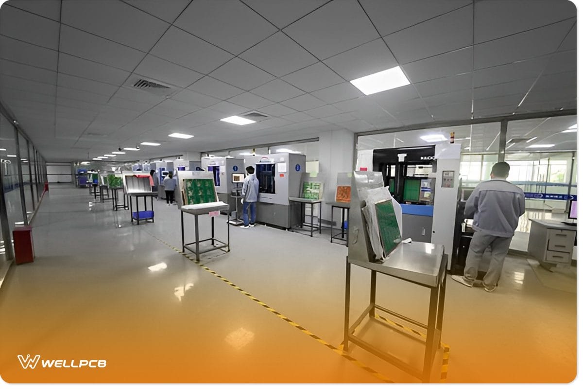
Industrial PCB Testing Equipment
The previous chapter highlighted some of the methods for manually checking PCBs to find faults.
In other cases, you might employ lenses and devices like a Multimeter,r for the same purpose.
Then again, when working as specialized manufacturers, these methods could become tedious. aily, you will be subjected to incredibly complex circuits with different specifications.
Under such conditions, unaided VMI becomes defective.
This chapter will look at some of those critical tools we use in industries when testing PCBs. Below are some of the devices.
The Automated Optical Inspection (AOI)
The fundamental requirement of PCB testing is to ensure that PCBs are produced to meet all the conditions included in their designs.
However, as I indicated in the introduction, sometimes errors are overlooked during production. OI machines help you scan a PCB and check for design irregularities.
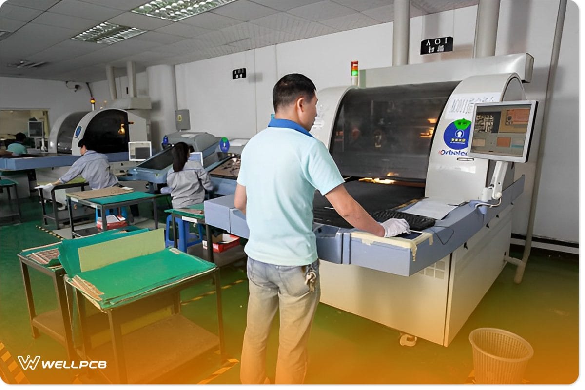
AOI machines aid Manual Visual Inspection (VMI) during PCB manufacturing. They consist of coordinating cameras and a platform for holding the PCB to be inspected.
The board is then lit from different specific angles as the cameras take image scans from the tips.
Using the images, AOI machines can construct an abstract representation of the PCB and compare it with the design specifications of the original PCB design.
These machines do some VMI faster and more accurately than could be done manually.
Automated Optical Inspection tools primarily focus on minimizing structural errors.
Currently, there exist both 2D and 3D AOI machines. Of the two types, the new 3D AOI machines perform faster and better than their 2D predecessors. They are also sensitive enough to detect significant power-related errors.
Advantages of AOI machines
- They are more popular than other machines
- Detect structural errors faster
- It can be utilized during manufacturing to minimize the overall time spent in final testing.
Disadvantages of AOI machines
- They cannot examine hidden connections or underneath BGAs
- They are ineffective when examining loaded boards with hidden components.
Flying Probe-Testing Machine
Flying Probe Testing machines (sometimes referred to as Flying Prototype machines) provide a platform for assessing prototype performance.
These machines differ from AOIs in performing some In-Circuit Testing of PCBs. Hey is preferred to older testing methods because they are cost-effective and easy to operate.
The Flying Probers consists of a board of pins interconnected to different components aboard. These machines perform rapid in-circuit testing to ascertain the effectiveness of prototypes.
The members then get tested by either powering or sending signals, assessing their inputs and outputs against those expected in their designs.
Advantages of Probe-Testing machines
- They are cheaper and faster than ordinary ICT testing machines.
- Increase quality as they allow engineers to produce prototypes and add changes to them before final releases.
- They are easier to operate than traditional ICT machines.
Disadvantages of Probe-Testing devices
- They are not detail-oriented like the conventional ICT machines.
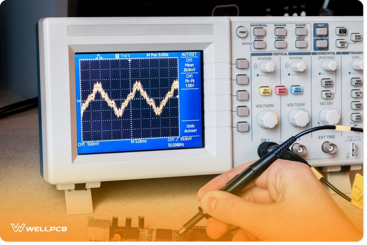
Impedance-Control Testing Machines
The physical design of a circuit on board and the amount of current passing through the board affect any AC circuit passing close to the same course.
Combining these effects and the resistance through the circuit forms the circuit’s impedance.
Impedance testing is often tedious.
You will need to determine the conductor length, the spacing between the circuits, the width and height of the conductor, and the appropriate time to measure impedance.
A Time-Domain Reflector (TDR) measures the impedance aboard. However, normal TDRs are not very useful in automated impedance testing.
Improved Impedance control testing machines are therefore employed when manufacturing PCBs on a larger scale.
Copper Thickness Testers & Hole Examination Machines
The copper thickness testers and hole examiners are reasonably related machines.
These tools are usually over-the-desk devices used to measure either the width of a drilled or the thickness of the copper layer interconnecting components.
A sample Copper Thickness Tester
A Copper Thickness Tester measures the thickness of copper. A typical Thickness Tester looks like the one shown in the image above.
A Hole Examination Machine
Hole examination machines estimate the diameter of holes by inserting pins with different diameters. A typical hole examination machine could look like the one shown above.
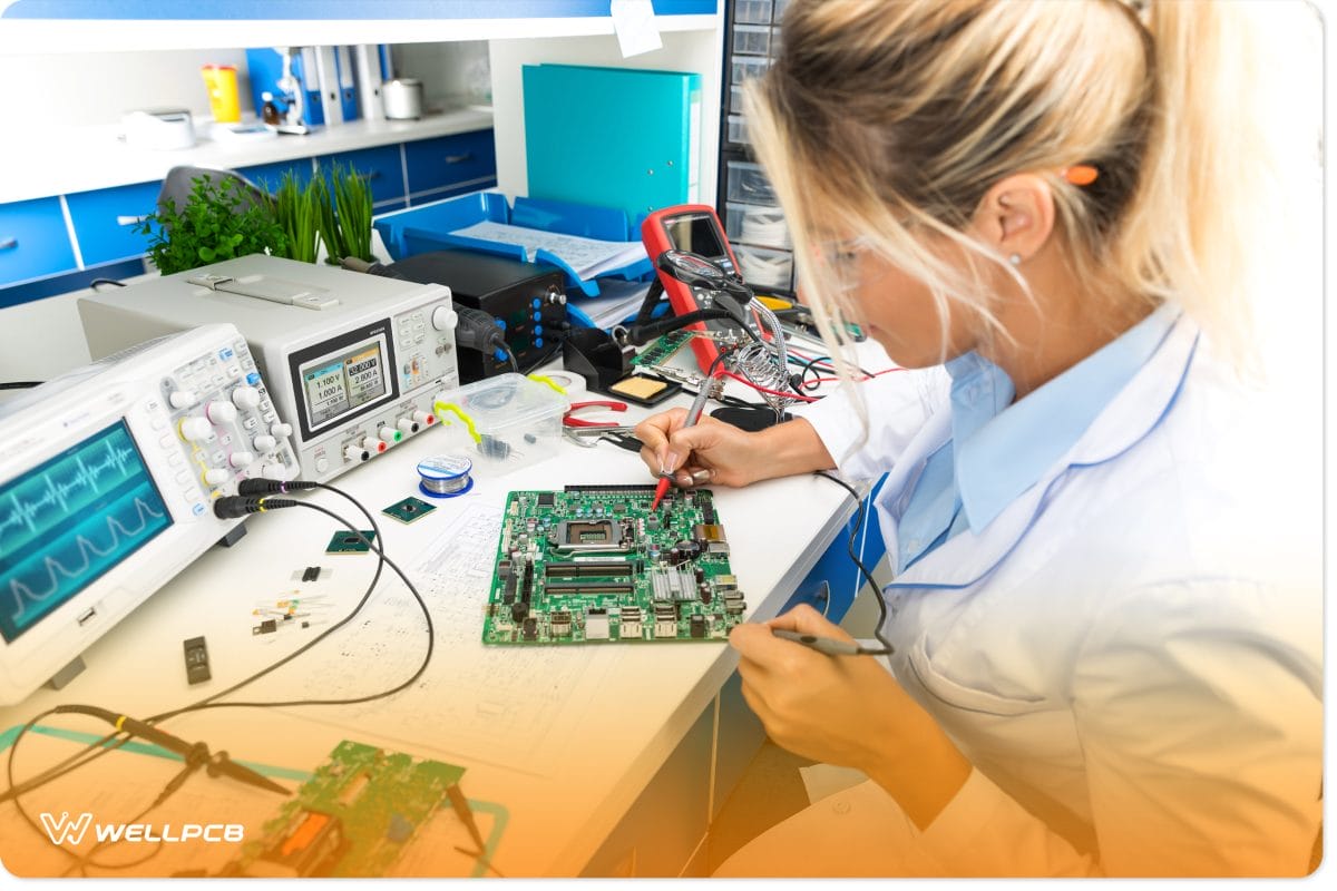
PCB Electrical Test Systems
Once all the components are welded onto the PCB, it is paramount to perform In-Circuit Testing and ascertain the efficiency of the integrated features.
Usually, this phase should come after a complete ICT.
Without comprehensive ICT testing, this type of testing can only indicate the probability of an existing problem without necessarily giving a way to locate or solve the error.
Generally, any other system developed to analyze the efficiency and reliability of a circuit board could fall under this categorization.
Chapter Overview
So far, we have highlighted the need to test PCBs and shown some of the machines used in the industry to test them. In the remaining chapters, we will now focus on the Assembly testing of PCBs.
PCB Assembly Testing
Introduction
Assembly testing of PCBs is a type of testing that is done after the electrical components specified in a PCB’s Bill of Materials (BOM) are fitted onto the board.
PCB assembly testing is closely linked to ICT (that we have already discussed before).
Usually, testing is done on a bed of nails fixed on a flat surface with access to multiple components connected at the PCB. Depending on the testing schedule, the board may or may not be powered. He A PCB’s
Bill Of Materials (BOM) gets fitted onto a board. CB assembly testing is done in two approaches:
- Testing a single component/module on board and investigating its correlation with every other component within the electrical components/modules network. His test is often performed for individual components and advanced to every other component within the network that shares interests with the tested element.
- Testing involves sampling a few specific critical components on the circuit and investigating the performances of the component(s)compared to the expected outcomes.
Benefits Of Assembly Testing
- An entire circuit board is tested for power faults, such as shorts or incomplete circuits. The test also establishes the presence of defective components on a prototype.
- This type of testing also involves power-up tests that help to minimize a customer’s debug needs significantly
- It can detect nearly all possible faults in a PCB
- Has an Operating System platform-independent PCB testing platform
- Testing follows accepted universal IPC standards
Demerits Of Assembly Testing
The main issue with Assembly testing is that testing a single prototype PCB takes time and financial resources.
Sometimes, trying a single complex board can take five to six weeks, and the cost of testing such a board can be very high.
Assembly testing is, however, functional and is more accurate when trying PCBs than any other testing method.
It is, therefore,e ideal for developed brands that require high standards of quality and massive productions.
Conclusion
Testing PCBs is a pivotal step for all PCB designers and engineers.
As the illustrations in this guide show, proper PCB testing techniques and approaches can directly impact the quality of electronics produced by an engineer.
Consequently, poor testing techniques are costly to businesses.
Therefore, because PCB testing directly impacts the quality of electronics produced by any company, it is worth every cent as it is directly linked to the overall profitability of any company.
The only problem is that most Contract manufacturers overcharge the testing of PCBs.
At WellPCB, we have equipped ourselves with the most modern methods of PCB testing equipment, and we take our time and expertise to test PCBs for our clients.
The last process of WellPCB will provide you with a one-stop service and high-quality products.
You can send us the documents you need to make and get a quote immediately!
What are we waiting for?
We have ten years of PCB manufacturing to check and test the specifications, requirements, and circuit problems again.
So, you will be satisfied with the PCB testing and quality. Alternatively, you can give us a quotation for your PCBs to be assembled and tested.