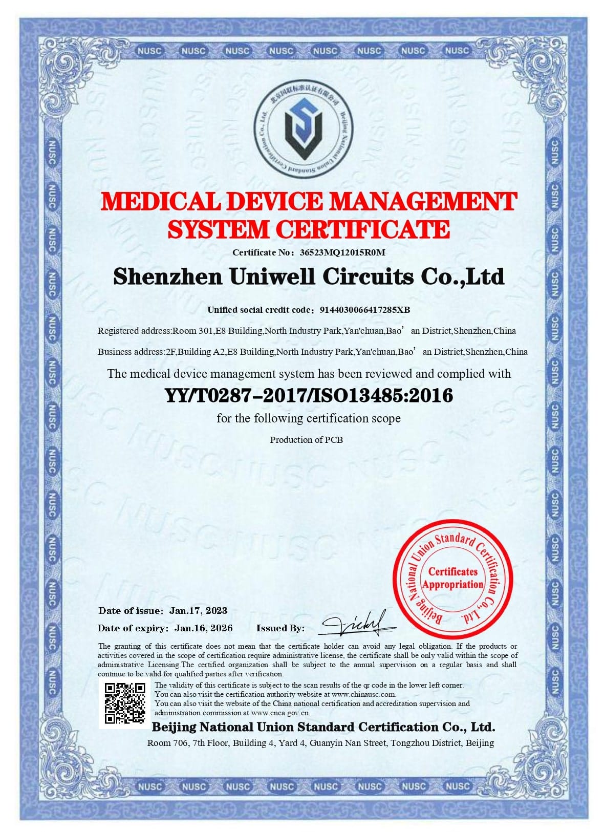
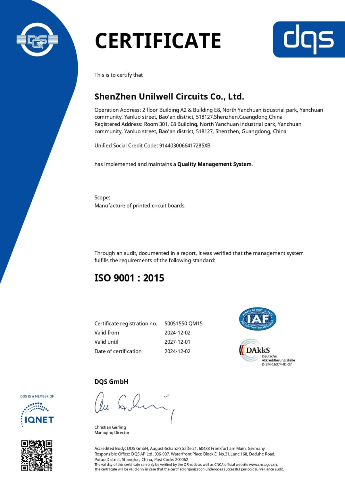
ISO9001 ISO13485
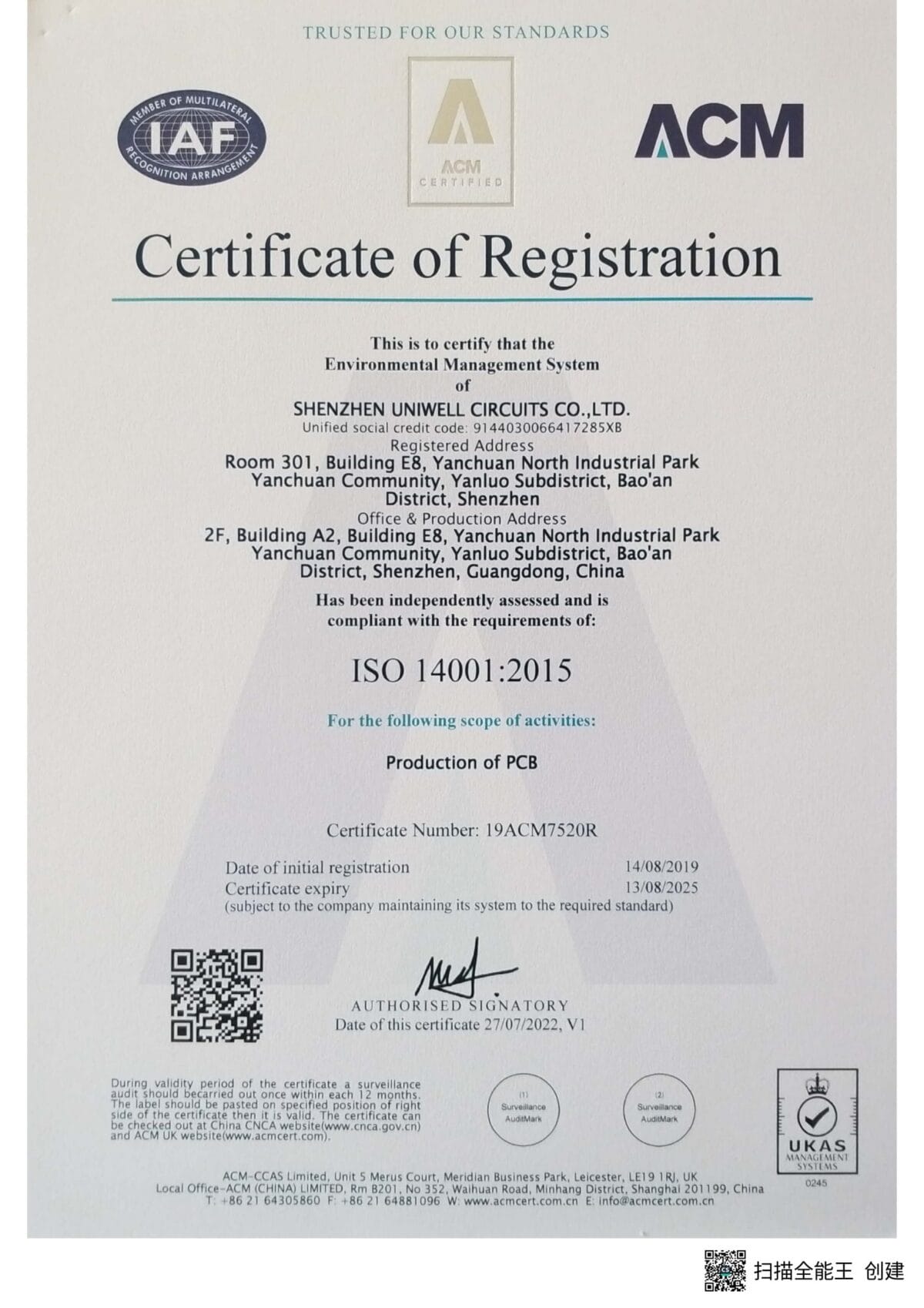
ISO14001

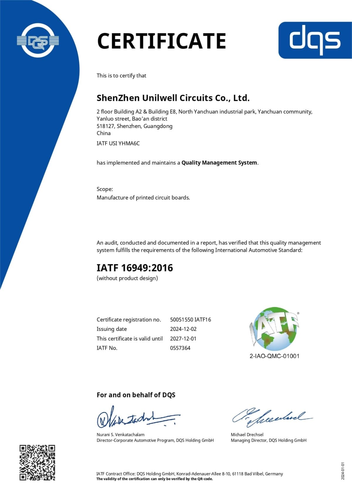
IATF
16949
IPC-A-610H International
Certification

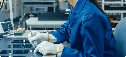
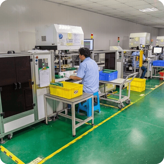
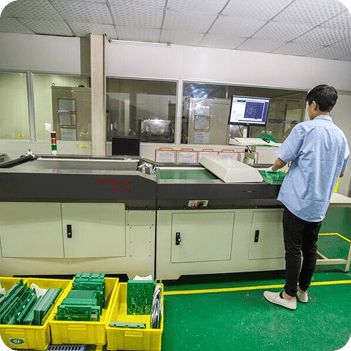
Fully Automated
AOI Inspection

Electronics and DIY Projects

Robotics

Home Automation

Art and Interactive Installations

Amateur Radio (Ham Radio)

Computer Building and Modification

Model Railroading

Music and Audio Synthesis

Easy Ordering for Hobbyists

Full Support from Design to Delivery

Fast Turnaround Time and Global Shipping

Industry-Leading Processes and Testing

Better Quality Than DIY Solutions

Access to Advanced Materials and Features

Faster Prototyping and Testing

One-Stop Fabrication and Assembly

Gerber files (preferred format)
.pcb, .pcbdoc, or .cam files if Gerber is not available
Notes or drawings indicating any special fabrication needs (such as solder mask color or silkscreen details)
Schematic to help verify the design
Bill of Materials (BOM) if you also want PCB assembly
Stencil design, if needed, for component placement

Submit Your PCB Design
Upload your Gerber files or use our easy online PCB design tool to create your board layout. Make sure your files are complete and correctly formatted to ensure smooth processing and production accuracy.

Select Your PCB Specifications
Customize your order by choosing the technical specifications—number of layers, board dimensions, thickness, copper weight, solder mask color, surface finish, and more. Our intuitive interface helps you configure everything based on your project’s needs.

Get an Instant Quote
Once your design and specs are in place, you'll receive a transparent, instant quote. Pricing updates in real time as you modify options, so you can adjust your selections to match your budget before placing the order.

Confirm Order & Make Payment
Review your entire order for accuracy, including file previews and selected specs. After confirmation, proceed to secure checkout and choose your preferred payment method. You’ll receive an email confirmation with order details.

Production & Delivery
Your PCB moves into production immediately. We’ll keep you updated throughout the manufacturing process. Once completed, your boards are carefully packed and shipped to your door, with tracking information provided for your convenience.

Engine and Powertrain Control
These PCBs manage functions such as fuel injection, ignition timing, and transmission control, where precision and reliability are required.
To withstand high vibration, temperature extremes, and mechanical stress, we use high-Tg FR4, metal-core laminates, and advanced solder materials. PCB designs follow AEC-Q100 testing principles, incorporating controlled impedance routing, optimized vias, and copper weights up to 20 oz to support high current loads and mechanical durability.
All boards pass thermal cycling between -40°C and +125°C and vibration testing to confirm durability in harsh automotive environments and comply with IPC-6012DA acceptance criteria.

Battery Management Systems (BMS) and Power Control Units (PCU)
Our PCB manufacturing processes apply advanced technologies such as HDI PCBs with microvias, thermal vias, and heavy copper options to manage high current loads and thermal expansion.
Materials include FR4, polyimide, and metal-core laminates for heat resistance and long-lasting performance. We optimize PCB design for high reliability, supporting critical functions such as cell monitoring, charge control, and thermal management.
To meet AEC-Q200 and IPC-6012DA standards, every PCB assembly undergoes thermal cycling from -40°C to +125°C, temperature humidity testing at 85% to 95% RH, and thermal shock test cycles.

Advanced Driver Assistance Systems (ADAS) and LiDAR
We use high-frequency laminates, such as Rogers and PTFE, to maintain signal integrity at high speeds.
Our PCB design incorporates controlled impedance routing, blind and buried vias, and tight trace tolerances to support reliable data transmission. All designs meet AEC-Q100 signal integrity and EMI/EMC performance criteria required for ADAS and LiDAR systems in autonomous driving applications.
For these sensors, we engineer PCB assemblies to withstand mechanical stress, thermal cycling between -40°C and +125°C, and high vibration up to 10G. Each printed circuit board undergoes AOI and X-ray inspection, plus functional testing, to verify accuracy and long-term reliability in real-world automotive environments.
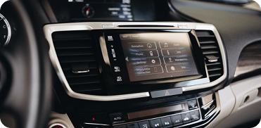
Infotainment and Communication Systems
Our PCB manufacturing uses high-density interconnect (HDI) technologies, flex PCBs, and rigid-flex configurations to support compact, lightweight designs while maintaining durability.
We select materials that withstand thermal expansion and contraction cycles and maintain the electrical reliability of circuit boards over long service lives. To comply with AEC-Q100 and EMI/EMC standards for high-speed data transmission, PCB assemblies include optimized grounding, controlled impedance, and EMI shielding to prevent signal interference.
Each circuit board is verified through AOI, X-ray, and functional testing to meet quality standards and performance-driven requirements for audio, video, wireless communication, and advanced 5G automotive applications.

Climate Control and Comfort Systems
Our PCB solutions for HVAC, seat heating, and cabin comfort controls use high-Tg FR4, metal-core substrates, and polyimide laminates to withstand extremely hot environments and changing humid environments.
Following IPC-6012DA Class 3 standards and AEC-Q200 environmental stress requirements, design considerations include expansion and contraction management, optimized thermal vias, and solder joint reinforcement to maintain durability. Each PCB assembly is tested for vibration, thermal cycling between -40°C and +125°C, and temperature humidity conditions of up to 95% RH to confirm the reliability of circuit boards exposed to mechanical stress and thermal fluctuations over time.


Hommer Zhao
Founder and Chief Editor – Hommer Zhao
Welcome! I’m Hommer Zhao, the founder and Chief Editor of WellPCB. With years of experience in the PCB industry, I’m committed to making sure our content is both accurate and helpful. We’re proud to serve a growing community of over 4,000 customers worldwide, and our goal is to provide you with the best resources and support. Your satisfaction is our top priority, and we’re here to help you every step of the way!

Jesse Holland
Technical Manager – Jesse Holland
Hi, I’m Jesse Holland, an Engineer and Technical Manager at WellPCB. With years of experience in PCB design and engineering, I’m here to ensure that every project we work on meets the highest technical standards. I lead our team, focusing on precision and innovation, collaborating closely with clients to provide tailored solutions and expert guidance. Whether you’re facing a complex design challenge or need advice on technical aspects, I’m here to ensure your project is a success from start to finish.

Nathan Jensen
Purchasing Manager – Nathan Jensen
Hi, I’m Nathan Jenson, the Purchasing Manager at WellPCB. I’m responsible for sourcing the best materials and components to ensure our products meet the highest quality standards. With my extensive experience in procurement, I work closely with suppliers to secure reliable and cost-effective solutions while maintaining strong relationships to support our operations. I aim to ensure every project runs smoothly by providing the resources needed to deliver on time and to your satisfaction.

Emma
Sales Manager – Emma
Hey, I am Emma, sales manager at WellPCB. I studied electronic science and technology at university and have served customers for PCB and PCB Assembly service for several years.
I enjoy communicating with customers and our technicians to solve problems, and customers always say, "It's great to have you onboard".
It is my pleasure and honour to be helpful. Contact me now, and you'll know.

Bella and Cassiel
Sales Representatives – Bella and Cassiel
We’re Bella and Cassiel, your dedicated sales representatives at WellPCB. With our extensive knowledge of the PCB industry, we’re here to provide exceptional service and support. We take the time to understand your unique needs and are always ready to offer tailored solutions and advice. Whether you need product recommendations, assistance with your orders, or simply have a question, we’re here to ensure your experience is smooth and seamless at every step.

Mandy and Wendy
Sales Representatives – Mandy and Wendy
We’re Mandy and Wendy, your friendly sales representatives at WellPCB. Passionate about helping our customers, we bring a wealth of experience in the PCB industry to provide you with the best solutions and service. We take pride in building strong relationships with our clients, understanding their specific needs, and offering personalised support to ensure their satisfaction. Whether you’re looking for advice, product information, or assistance with any part of your order, we’re here to make your experience as smooth and efficient as possible.
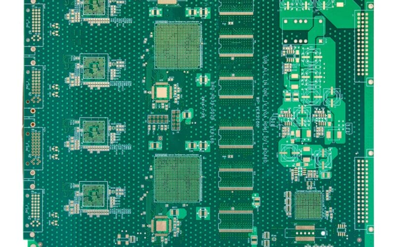
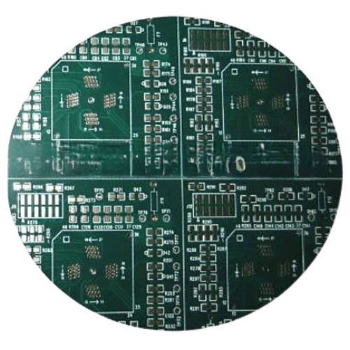
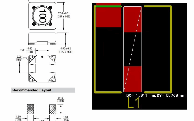
PCB Specifications
- Layers: 8
- Board Thickness: 1.8mm
- Min. Line Width/Space: 3/3.5 mil
- Min. Hole Size: 0.2mm
- Min. Distance from Hole to Line: 0.13mm
- Inner Layer Copper: Hoz
- Outer Layer Copper: 1oz
- Surface Finish: Immersion Gold
The final board met all mechanical and electrical tolerances and passed electrical testing with 100% yield. This project shows our capabilities to handle complex, high-density multilayer PCBs with tight tolerances and strict quality standards.
Project Details
- Service Type: PCB Assembly
- Location: Italy
- Client Type: PCB Design Company
- Total Units: 20
- Lead Time: Rapid turnaround for prototyping
- Assembly Type: SMT+THT mixture assembly
Our experienced production team worked closely with the client to verify the BOM, optimize the stencil and the board’s layout design. We completed and delivered 20 fully assembled units within the expected lead time, allowing the client to avoid delays and meet their customers’ delivery window. This case highlights our capabilities to support global clients with flexible, low-volume PCB assembly solutions.
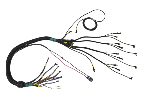
Project Details
- Service Type: Custom Automotive Wire Harness
- Location: New York, USA
- Client Type: Auto Repair Shop
- Quantity: 10,000 Units
Our team followed strict quality guidelines throughout production, using automotive-grade connectors and insulation materials. The order was completed on schedule with no reported defects, supporting the client’s rollout without interruption. This case shows our comprehensive capabilities in large-scale production, customized solutions, quality control and efficient delivery.