
About PCB Material. In PCB manufacturing, you need to consider how to choose the right material for your PCB design.
There are many different types of materials, each with different characteristics. For example, we need to consider design implementation and cost.
This guide can help you learn more about the various materials and how to choose PCB materials for your board?
Let’s get started.
Contents
1. PCB Material Types
1.1 What Is PCB?
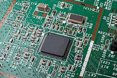
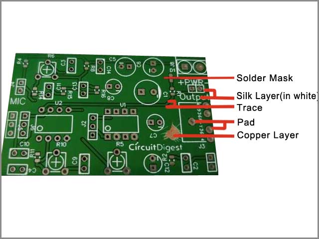
A copper-laminated and non-conductive printed circuit board (PCB) is very useful in which all electronic and electrical components are connected in one common board with internal connections.
PCB design circuits are very complicated because connections between circuits are built through the wires which makes the circuit complexity and complicated.
So after designing of PCB the circuits becomes very easy to understand and flexible because now there is no need for wires, it makes the internal connection between the components and assembles quickly.
Also, it reduces the complexity of the circuits. The requirement of the user can design the PCBs. It can be founded on many devices like TV, mobile, digital camera, computer parts like graphics cards.
If you talk about the PCB material, the name which comes to know is Rogers. Rogers has been the material for advanced electronic PCB material.
A dielectric material is a substance that is a poor conductor of electricity and is used as an insulating layer in the PCB build-up. Porcelain, mica, glass, plastics, and some metal oxides are good dielectrics.
The lower the dielectric loss, (the proportion of energy lost as heat) the more effective the dielectric material.
If the voltage across a dielectric material becomes too high — that is, if the electrostatic field becomes too intense — the PCB material will suddenly begin to conduct current. This phenomenon is called dielectric breakdown.
Rogers 4350 is less likely to demonstrate a dielectric breakdown condition than FR-4.
The best part of this industry is when advanced electrical properties and performance are critical to your designs, Rogers’s materials provide:
1. Lower Dielectric loss
2. Low electrical signal loss
3. A wide range of Dk (dielectric constant) values (2.55-10.2)
4. Low-cost circuit fabrication
5. Low outgassing for space applications
1.2 PCB Material Types
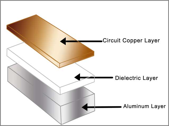
1.2.1 Aluminum PCB
The basic construction structure of an IMS PCB includes: the ic layer will perform as the conducive link between IC and heat sink. Unlike FR4. The copper and aluminum foil material is placed at the bottom, then the composite resin material which is an electrical insulator but thermally conductive, finally at the top the copper foil or laminate, and then pressed under high pressure and temperature.
Common PCB thickness is 1.6mm, 100µm ceramic isolation layers, and 35µm copper foil over the insulation layer. The tracks are made of the copper laminate layer. Components are also placed and soldered on the copper layer side.
We often divide Aluminum constructions into mainly three layers.
Circuit Layer: It is a copper layer that comes with a thickness of around 1 to 10 oz.
Insulating Layer: A dielectric layer of thermally conductive and electrically insulating material
Base Layer: This is mainly composed of copper or things that you need to consider when determining the best layout. Options such as an aluminum metal substrate. There are multiple thicknesses available. However, the most common one is 1mm.
The aluminum PCB is further divided into subcategory:
- Flexible aluminum PCB
- Hybrid Copper core PCB, or a mixture of specific metal alloys.
However, the aluminum PCB - Multilayer aluminum PCB
- Through Hole aluminum PCB
You can use these different types in different applications.
Advantages of Aluminum PCB
If you compared aluminum PCB with the other PCB material it has many benefits, i.e.:
- The Aluminium is a low-cost metal and available
- Its processing cost is also low. The final products are low priced.
- The Aluminium PCBs are environment-friendly, the excellent heat dissipater, more durable and lightweight.
- By a mechanical point of view, they are more rigid and reliable, increase product life and durability.
- From the electrical point of view, they are excellent in EMC-EMI shielding characteristics.
Applications of Aluminum PCB
►These products were developed for high-power switching applications, but they gained enough popularity when they introduce LED applications.
►The aluminum design operates at a higher current for mounted LEDs, keeping the temperature tolerance within specified limits.
►The automotive and RF industries go the extra mile to utilize the advantages of these products and make them available for the common man.
►Aluminium PCBs are a valid choice for applications involving heat dissipation because they provide an ideal exit of the heat with the help of dielectric, maintaining the overall temperature of the project design.
1.3 Other Material Types
Now you can easily compare the aluminum PCB with other materials listed below:
1.3.1 FR4
FR-4 PCB stands for Fire Retardant or Flame Retardant level 4. It is a suitable insulator material so does not conduct the current. That is a glass-reinforced epoxy laminate composite material or woven glass with epoxy resin.
A fundamental component of a PCB is an FR-4 PCB panel sheet laminated with a thin layer (such as 17µm, 35µm, or 70µm) of copper on at least one side or both sides.
The FR-4 material due to its fire-retardant properties replaced its predecessor G-10 material which lacks the self-extinguishing properties.
The relative permittivity is 4.4, dielectric strength is 5MW/m, and the electrical breakdown is 50kV. The glass transition temperature or Tg is another characteristic where the substrate changes its electrical properties abruptly, FR-4 PCB has 140°C Tg.
The Tg varies the substrate from a glassy or resin substrate to softer and rubbery material.
The FR-4 material provides the base standard for PCB substrates, delivering a widely useful balance between cost, manufacturability, electrical properties, durability, and performance.
As you know that everything has specifications and certain limitations, so FR4 also has certain limitations which are given below:
►Er (dielectric constant) stability from lot to lot and over frequency is one of them.
►The loss is another, then there is the concern of lead-free processing temperatures, and perhaps thermal conductivity as even low-power RF can consume much power if the active circuits are biased to provide very high linearity.
When ordering an FR-4 PCB or PCB fabrication, the thickness of copper over this material should also be mentioned. As high current circuits need thick, full copper tracks and the opposite is true for low current circuits. The default thickness of a PCB material is 1.6mm.
Wne use FR-4 PCB for low-frequency signals, whereas lower dissipation materials for high-frequency signals such as antenna design, RF and microwave applications.
Other than this FR4 is commonly used in PCB material because of its efficiency. Some of the other qualities of FR4 are given below:
|
FR4 |
Glass transition temperature | |
|
standard |
130 |
►Most commonly and widely used ►cheapest |
|
Higher glass transition |
130-170 |
►Perfect with the lead-free reflow innovation |
|
Halogen-free |
– |
1.3.2 FR1 And FR2
|
FR1 |
FR2 | |
|
Made up of |
Phenol and paper compound |
Phenol and paper compound |
|
Glass transition temperature |
Higher temperature, used in single layer PCB |
Low temperature, used in single layer PCB |
|
These materials are halogen-free, and non-hydrophobic |
These materials are halogen-free and non-hydrophobic |
CEM-1 AND CEM-3:
|
CEM-1 |
CEM-3 | |
|
Material |
paper and two layers of woven glass epoxy and phenol compounds |
white colored, glass epoxy compound |
|
Usage |
Use in single-sided PCB |
Use in double-sided PCB |
|
Price |
Higher price than FR4 |
Lower cost than FR4 |
1.3.3 Polyimide
We often use this material in flexible PCB. This is made up of keeping on, Rogers, DuPont. This material has excellent electrical properties and a wide temperature range. The working temperature range is 200-300 degrees centigrade.
1.3.4 Prepreg
Prepreg stands for pre-impregnated. It is fiberglass impregnated with resin. These resins are pre-dried so that when you heated it flows, stick, and are immersed.
Prepreg is a similar adhesive layer to the FR4 which gives the strength. According to the resin content, there are many versions of this material SR- standard resin, MR- medium resin, and HR-high resin.
The version is chosen according to your layer structure, thickness, and quality impedance. This material is also available as halogen-free and high glass transition temperature.
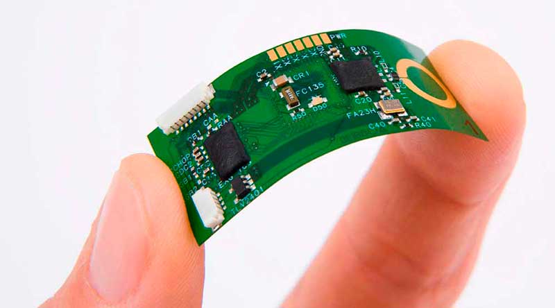
2. Flexible PCB Material
2.1 What Is A Flexible PCB?
Flexible PCB is a type of PCB as you know that before. The WellPCB offers DC motor controllers in both domestic and international markets. We have a flexible PCB material is also sub-divided into single-layer, double-layer and flex PCB. The flexible PCB is made up of loose and flex material such as plastic.
The advantage of the flexible material is you can turn or shift the PCB without damaging the components or any other connections.
2.2 Flexible PCB Material
You studied that every component has layers. Similarly every PCB consist of three layers
►Base material
►Bonding adhesive
►Metal Foil
Base Material
Wne use the polymer film as a flexible base material which provides the foundation of the laminate. You can see that most of the times under normal circumstances the base material provides the very essential physical and electrical properties to the film.
In that circuits where the bonding is less strong, the base material contains all the characteristics to the film. The base material is present both in thicker film and thinner film.
The range of thicker film is between 12µm to the 125µm, but thinner films are more flexible to use because you can quickly move the film. You can also say that‘Stiffness Increases Is Proportional To The Cube Of The Thickness.’
Means that if you doubled the thickness, the stiffness becomes also increases 8times but the effect will deflect by 1/8 times.
Bonding Adhesive
It is used as a bonding medium for creating the laminate. When it comes to the temperature, the properties become changed.
When this problem is reported, then different kind of adhesive materials introduced with the different thickness. Applications of this film are dependent upon the adhesive thickness.
Metal Foil
The most common and most widely used layer because each of the components is attached to this layer. The copper layer is very vastly used for this purpose.
As you already know that there are various types of copper films are present in the market. You can easily choose the thickness of the film as per you are required.
3. PCB Material Properties
PCB material properties are listed before, and now you can easily understand the impact of these properties.
3.1 Criteria For Selecting The PCB Material
While selecting the material for your PCB, two principal properties are to be considered. Whenever you have to choose the PCB, you have to think these significant requirements.
►Thermal properties
►Electrical properties
Thermal and electrical properties are further divided into many small properties which are very important for the selection of PCB material, you have to consider these factors also. The properties are below:
Thermal Properties
- Thermal conductivity (K)
- Decomposition temperature (Td)
- Glass transition temperature (Tg)
- The coefficient of thermal expansion (CTE)
Electrical Properties
- Electrical strength of a PCB material
- Volume Resistivity
- The surface resistivity of a dielectric material
- Loss of tangent/dissipation factor
- Relative permittivity/dielectric constant
3.2 Thermal properties
• Thermal Conductivity (K)
Thermal properties lead to the heat conductivity of the material, means that how good is your material to resist the heat. The units for measuring the thermal properties are watts per meter Kelvin (W/Mk).
Commonly the thermal conductivity range is 0.3-6 (W/Mk) in dielectric materials. Copper is an excellent thermal conductor because its thermal conductivity is near to 386 (W/Mk) and it can transfer heat at the high rate than the dielectric PCB layer.
• Decomposition Temperature (Td)
Decomposition of PCB starts when PCB substrate is exposed to the temperature and crosses a specific threshold level.
Decomposition temperature is the range within which the decomposition substrate occurs. This reaction is not reversible even though the substrate is experienced the low temperature.
Therefore it is essential that you select a PCB material which can bear the temperature of the room where you are working. Preferably it is recommended that the material which can bear 250-degree centigrade. 200 to 250 degree Celsius is the required temperature for the solder of PCB.
The glass transition temperature is below the range as compared to the glass transition temperature which is higher than the range.
• Glass transition Temperature (Tg)
The glass transition temperature and the decomposition temperature is much similar the significant difference is when the PCB substrate is exposed to the temperature the threshold level is beyond and starts to soften.
It is a reversible reaction because when the substrate is cooling down, it easily achieves the previous shape. So we can say that substrate can transform from one form to the other and this is the range of glass transition temperature.
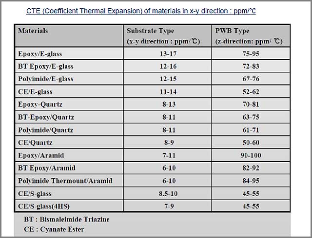
• The Coefficient Of Thermal Expansion (CTE)
The expansion rate of PCB is known as the coefficient of thermal expansion (CTE). The measuring units are parts per million (PPM).
The CTE may be increased or decreased depending upon the temperature variation on the substrate. Here is the question arises that when the temperature of the substrate increases and when it drops?
The best answer is that the CTE is increased when the temperature of the substrate increased beyond the glass transition temperature. There exists a difference in CTE between the copper layers and substrate.
The copper layer is used everywhere for the coating purposes, but there is a drawback, the copper layer generally has the lower CTE than the substrate, so when heating is applied, they face the problems of interaction which is caused by the difference between the two layers.
The CTE of PCB on 2D coordinate system is maintained at a range of 10 to 20 PPM, but the minimum CTE should be kept. The best CTE for use is 70 PPM or below.
3.3 Electrical properties
• Electrical Strength Of A PCB Material
Electrical quality of a PCB is characterized as the capacity of the material to oppose disappointment or even a breakdown in the electrical framework on Z course of PCB. The units used to measure electrical resistance is volts/mil.
In most of the cases, the range of the electrical resistance of PCB material is from 800 volts/mil to the 1500 volts/mil. The PCB should have the sufficient electrical strength.
• Volume Resistivity
Volume resistivity, the ability of the dielectric material to resist electricity or insulation. It is measured in Ω/m or Ω/cm.
It is crucial that we used PCB materials with high volume resistivity ranges from 10 MΩ/cm, also that dielectrics with high volume resistivity are preferred as compared to the low volume resistivity. The resistivity of the material can be affected by the moisture, cold and heat.
• The Surface Resistivity Of A Dielectric Material
That is the ability of a surface to resist electricity and insulation. Megaohm per square is used as a unit. The best range of this property is ranging from 103 to 109 MΩ/square. Temperature (high/low both) and moisture affect the surface resistivity.
• Loss Tangent/Dissipation Factor
It is straightforward to understand that when you say that
POWER LOSSES α LOSS TANGENT
Interpreted as if the power losses are low then the loss tangent is also small due to the direct relationship. Loss tangent is also dependent upon the frequency.
In between these, also direct relation is present. Whenever frequency increases the loss tangent also increases, this property is best between 0.02 and 0.001.
• Relative Permittivity/Dielectric Constant
Signal integrity and impedance are the two factors that affect the dielectric constant. It also depends upon the frequency, but the relation looks like this:
Dielectric CONSTANTα 1/FREQUENCY
Means that with the increase of frequency the dielectric decreases or vice versa. The best range is between 3.5 to 5.5.
Whenever you are using a material in the applications that utilize the high frequencies that should have the stable dielectrics with the full range of frequencies. It is essential for the safety purposes.

4. PCB Containing Material
In the high-speed world, the technology limited our life too, as you can see that many things will gather and it makes one useful element. High-speed digital is the example. Digital signaling requiring is high-frequency design to maintain the signal integrity.
To use the signal in the best quality has a rule of thumb, which says that.
Td>Tr/4
Td = time delay
Tr = rise time
Due to the high speed networking the high-speed digital signaling is required in the routers, servers, power applications, storage area networks and related appliances, this is because of the required high data rates.
While the increasing rate of growth and usage of data rate also uses the higher storage platforms or high-speed hardware’s. If we compared the RF/microwave with the HSD, we came to know that RF uses only a few layers of PCBs instead of it the HSD uses up to 20 layers.
Instead of this advantage, sometime PCB affect the system. There are different parts of the PCB like:
► Resins
► and Copper foil and other, which may affect the HSD quality of signaling.
5. PCB Substrate Material
PCB has two layers of material. One is the upper layer, and the other one is the lower layer. As we know that the top layer is vital for the reactions and other purposes and all of the PCB designing is dependent on that film.
Likewise, the lower layer is also significant for the designing purposes. If you estimated the worldwide substrate market, it is approximately equal to the 51 million square.
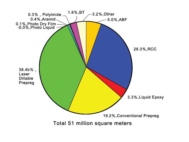
Majority of the substrate materials will mix with epoxy, and some of them will combine with BT mixture. The majority of the market uses the alternate layers of the dielectric PCB material, with or without reinforcement are stacked at the metal foil to form the PCB.
The below chart will give you the best idea for the selection of the substrate:
There are three basic PCB material types are present:
• The non-woven glass contains a dispersion of glass microfibers in the substrate. They only work at the higher frequencies, but the dispersion factor is not good.
• Woven glass made up of weave glass cloth, but this is not good for use, because it has poor mechanical and thermal stability at the multilayer design.
• Filled has a specific range of dielectric constant. Also, other materials like ceramics are for increasing the scale of the dielectric constant.
6. How To Choose PCB Materials Of Your Board
Different types of PCB materials are available in the market today. However, finding good quality of these materials could be a challenge especially if you lack sufficient knowledge on the criteria to follow when selecting PCB materials to use. This article will provide you with the information you require to settle for the right PCB materials.
6.1 Criteria For Selecting Materials To Be Used In PCB Boards
The factors to consider when selecting materials used in PCB can be categorized into two main classes: thermal properties and electrical properties.
6.1.1 Thermal Properties
· Thermal Conductivity (k)
The ability of PCB materials to conduct heat is referred to as thermal conductivity. A materials thermal conductivity level determines its ability to transfer heat. The thermal conductivity of a material is measured regarding Watts per Meter at Kelvin (W/Mk). In most dielectric materials, thermal conductivity is within the range of 0.3 W/Mk to 6W/Mk. Copper has a thermal conductivity of 386 W/Mk. Due to its high thermal conductivity, it can transfer heat at a higher rate than PCB’s dielectric layer.
· Decomposition Temperature (Td)
When a PCB substrate is exposed to temperatures that exceed a given threshold level, it tends to decompose. Decomposition temperature is the range within which decomposition of the substrate occurs. Once decomposition of the substrate has occurred, it cannot be reversed even when it is exposed to low temperatures. It is, therefore, necessary to select a PCB material that can withstand the temperatures range in which you work within. It is recommendable to choose a material that can withstand temperatures above 250 0 C. To solder the PCB substrate, a temperature range of between 200 degrees Celsius to 250 degrees Celsius is required. The decomposition temperature should be above that range while the glass transition temperature should be below the range.
· Glass Transition Temperature (Tg)
When a PCB substrate is exposed to high temperatures beyond a given threshold level, they tend to soften. When the substrate is cooled, it gains the initial state it had before heating. Glass transition temperature is the range within which a substrate can be transformed from one form to the other.
· The Coefficient Of Thermal Expansion (CTE)
The expansion rate of PCBs is referred to as the Coefficient of thermal expansion. It is measured using the units of parts per million (ppm). The coefficient of thermal expansion may increase or decrease depending on temperature variations on the substrate. For example when the temperatures to which a substrate increase beyond its glass transition temperature, there may be an increase in the material’s coefficient of thermal expansion.
There exists a difference in CTE between the copper layer and the substrate. The copper layer generally has a CTE lower than of the substrate. When heat is applied, there may be problems of interconnection due to the difference in CTE between the two layers. The CTE of PCB on both the X and Y axis is maintained at a range of between 10 to 20 ppm. The minimum CTE should be maintained. The recommended CTE is of about 70 ppm or below.
6.2 Electrical Properties to consider
· Electrical Strength Of A PCB Material
Electrical strength of a PCB is defined as the ability of the material to resist failure or even a breakdown in the electrical system on the Z direction of PCB. A PCB should have sufficient electrical strength to enable it to resist a breakdown in the electrical system. The unit for measuring electrical strength is Volts/mil. In most cases, PCB materials will have an electrical strength ranging from 800V/mil to 1500V/mil.
· Volume Resistivity
Volume resistance is defined as the ability of the dielectric material to resist electricity or insulation. It is measured in Ohms-meters or ohms-centimeters. PCB materials should have a volume resistivity of between 10 Mega ohms-centimeters. Dielectric materials with high resistivity are preferable as compared to those with lower resistivity. A material’s resistivity can be affected by external factors such as moisture, cold and heat.
· The Surface Resistivity Of A Dielectric Material
Surface resistivity is defined as the ability of the surface of the dielectric material to resist electricity and insulation. The unit used to measure surface resistance is Mega ohms per square. Dielectric materials with high surface resistivity are preferable. A surface resistivity ranging between 10 3 and 10 9 Megaohms per square is preferred for most dielectric materials. Surface resistivity is also affected by external factors such as moisture and high and low temperatures.
· Loss Tangent Or Dissipation Factor.
A dielectric material with low loss tangent has fewer power losses. In most PCB materials, loss tangent ranges between 0.02 and 0.001. Loss tangent increases with increase in frequency.
· Relative permittivity Or Dielectric Constant
The dielectric constant of a PCB material is significantly affected by signal integrity and impedance. It also depends on frequency. An increase in frequency results in a decrease in dielectric constant. The usual range of dielectric constant of a PCB material falls within the range of 3.5 to 5.5. A material to be used in applications that utilize high frequencies should have the dielectric constant which is stable on a wide range of frequency. That is very important for safety. Dielectric constant varies more in some materials than in others.
6.3 Impacts of heat and power on the selection of PCB Materials
Heat and power are major factors that affect the selection of PCB materials. These include;
· Absorption Of Moisture
The ability of a PCB dielectric material to withstand exposure to moisture is referred to as Moisture Absorption. In most cases, PCB dielectric materials will have moisture absorption ranging from 0.01% to 0.20%.
Moisture absorption of a PCB material affects the dielectric’s thermal and electric properties.
· Flammability
By Standards for Safety of Flammability of Plastic Materials for Parts in Devices and Appliances (UL94), plastics flame retardant features are categorized from high plastic flammability to low plastic flammability. According to UL94, it is a requirement that specimens of PCB materials should not burn with flaming combustion for more than 10 seconds.
· Methylene Chloride Resistance (MCR)
Methylene Chlorine Resistance in PCB materials is also referred to as chemical resistance. MRC is used in measuring the ability of the dielectric material to resist absorbing Methylene Chloride. In most dielectric materials, the Methylene Chloride Resistance ranges between 0.01% to 0.20%.
6.4 Mechanical Properties of Flex and Flex-Rigid Boards:
Some of the mechanical properties considered include;
· Density
The unit used to measure the density of a dielectric is grams per centimeters cubed. It can also be measured using pounds per cubic inch.
· Peel Strength
Peel strength of a PCB material is defined as the ability of copper layers and dielectric material to bond. Manufacturers can test the peel strength of PCB material by exposing copper traces with the thickness of one ounce to high temperatures, chemicals, and heat stress.
· Time To Delamination
It refers to the period a dielectric material resists delamination effects. When fiberglass and laminate materials are exposed to moisture or heat stress, they delaminate. The time duration these PCB materials take to separate from each other under moisture or thermal shock conditions is referred to as the time to delamination.
· Flexural Strength
The term Flexural strength refers to the tendency of dielectrics not to break when subjected to physical strength. The unit used to measure flexural strength is Pounds per square inch or Kilograms per square meter. There are two ways used in measuring the flexural strength of PCBs;
- By exerting force at the center of the board with the ends supported.
- By use of tensile modulus / Young’s modulus.
6.5 Other Factors To Consider In Designing PCBs. FR4
· The Thickness Of Boards Is Another Factor To Consider
Thickness influences the strength of boards. Thicker boards provide greater support when connecting heavy objects to the boards. For plane layers, the standard thickness of copper is 35 microns. Grams and ounces can also be used to indicate Copper thickness. Boards with a copper thickness more significant than the ordinary are better since they support a wide range of applications. In some cases, tracks may transfer power even though they are not meant to. It happens when signals fail to handle frequencies properly, and it may lead to tracks losing high power quantities.
· Track Distance
The most appropriate track distance for layer boards consisting of materials with copper tracking is two inches and the suitable time for signaling is one nanosecond. It is essential to put into consideration the impacts made by transmission line on long tracks especially when the integrity of the signal is important.
· The Condition Of The Vias
Most boards have the vias empty such that you can easily see through them. To create a protective barrier against impurities such as dust, the via must be filled. That is done to increase their capacity to conduct current.
Ball Grid Array abbreviated as BGA, and its pieces are used to fill the vias. When BGA pin comes into contact with the inner layer, solder is likely to fall and penetrate to the other layers through the via. Vias should, therefore, bne filled to prevent leakage of solder and to maintain the contacts quality.
· Strength And Durability Of The Material
The different materials used to develop a particular board should be strong enough to stay intact even when an electronic device accidentally falls or gets knocked from the sides. Most businesses and consumers are mainly concerned with reliability in all devices that have circuit boards. All types of PCB materials used on any particular board should be of high quality and reliable.
When selecting materials to be used in developing PCB boards, it is important to consider quality as the priority. Quality plays a major role in determining the performance and the lifespan of an electrical device. It does not matter whether the PCB is for home devices or industrial use, costly or cheap, large sized or small sized, the quality is the key factor to focus.
With long lasting PCBs, it is possible to make hardware updates even on computerized devices without interfering or damaging the materials that makeup PCB boards. Other household devices such as microwaves and electronic gadgets can last longer in good condition. For example, ATMs and other Electronic devices in public facilities remain in good working condition, with their buttons functioning correctly without fail.
· Cost
High-quality substrates with high frequencies are expensive but durable. It is, therefore, necessary to select a material of high quality bearing in mind that cheap can also be expensive.
With all the factors mentioned above put into consideration, it is necessary to select materials that suitable for use with high frequency. The substrate’s dielectric constant should be low while the foil should have the capacity to maintain low resistance.
Conclusion
At the end of this discussion, you are now well aware of the PCB requirements and effects of the environment on this. So from now on, you can select the best PCB material for your project which provides you the best quality results and also long-lasting effects.
WellPCB is the place to get the best PCB manufacturing and assembling services. Our expert team gives your project an ultimate manufacturing experience using FR4, Rogers, and other high-quality materials that are favorite in the industry.
For more information on PCB materials and other topics of interest, you can contact our support team at sales@wellpcb.net.